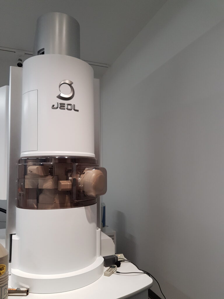
JEOL neoARM Scanning Transmission Electron Microscope. Probe Corrected. 30-200 kV. EELS and EDX
Transmission Electron Microscopy (Located in EER 0.750)
-Accelerating voltages at 30 kV, 80 kV, and 200 kV
-Probe Correction for atomic resolution Scanning Transmission Electron Microscopy (STEM)
-Atomic-level elemental mapping (EDS and EELS)
-Auto tune for fast alignment
-Chemical binding state and plasmon mapping (EELS)
-Energy filtered imaging
-Magnetic field mapping
Specifications
-Imaging Modes: TEM/STEM
-STEM resolution: 0.0783 nm (200 kV)/0.1108 nm (80kV)/ 0.1920 nm (30 kV)
-Energy resolution : sub 0.3 eV
-Point to Point Resolution TEM: 0.023 nm (200 kV)
-Source: Cold Field Emission
-Tilt Range: ± 80° (with high tilt holder)
Detectors and spectroscopy
-Hybrid high angle annular dark field detector
-Annular bright field detector
-Gatan One-View Camera with IS video software (up to 300 fps)
-Quantum Detectors Merlin Medipix2 Direct Electron Detector for 4D-STEM
-JEOL large angle silicon drift EDS detector (0.96 sr)
-Gatan Quantum energy filter with DualEELS
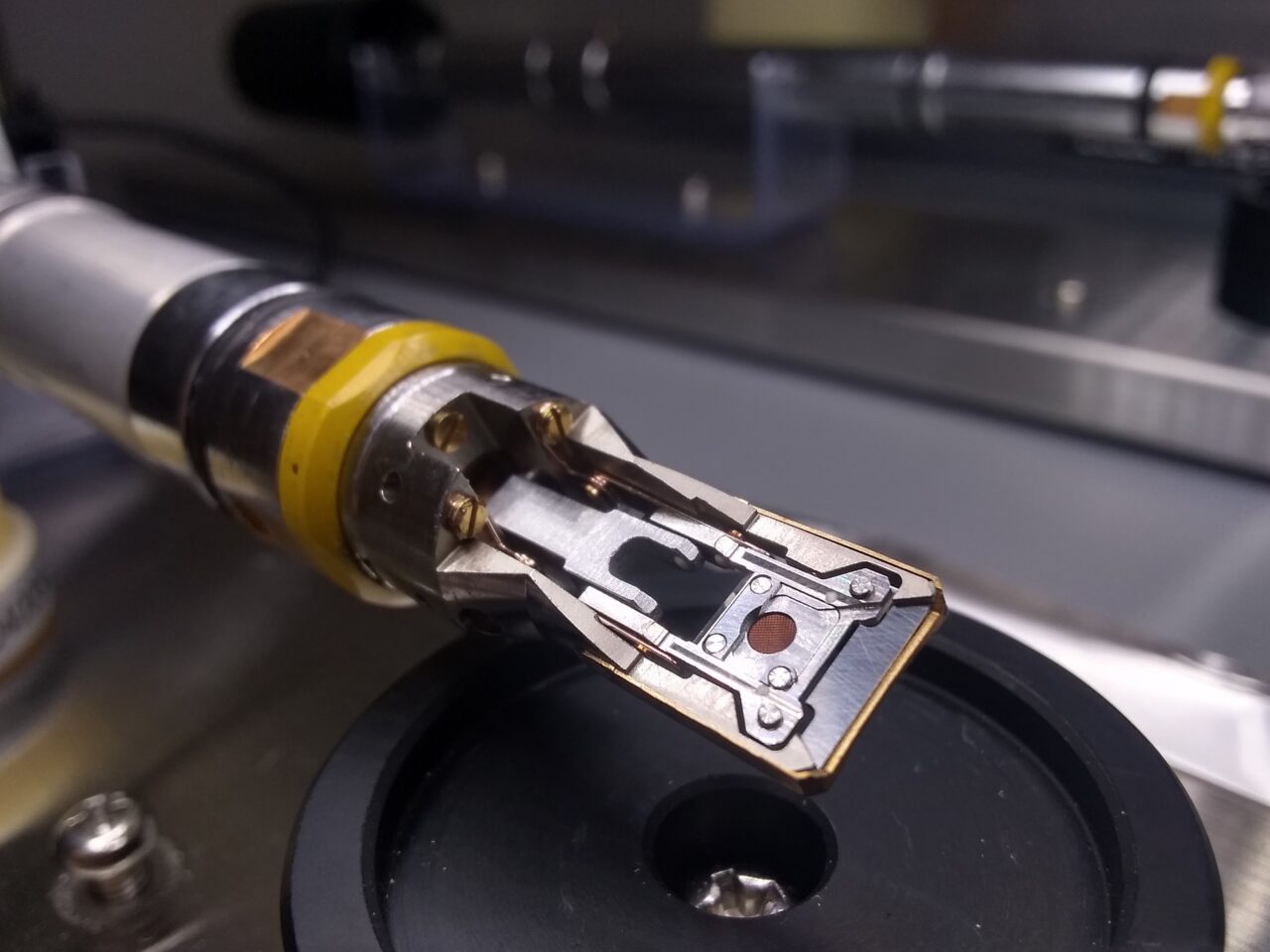
-Protochips Aduro heating/biasing holder
-Protochips Poseiden Liquid Flow Holder: Electrochemistry pack and Heating pack
-Gatan Elsa Liquid Nitrogen Cryo-TEM holder
-High tilt holder
-Double tilt Holder
—————————————————————————————————————————————————————————————————————————–
TEM access details
Access is available to the JEOL neoARM TEM at a rate of $120 /hr, which includes the provision of an experienced TEM operator.
- Hourly fees
- Trained On-Campus UT Users: $120/h.
Facility User Education
To become a user of this instrument please contact Professor Jamie Warner to schedule a training session. Email: jamie.warner@austin.utexas.edu
—————————————————————————————————————————————————————————————————————————–
Example results
Cutting-edge techniques for materials characterization are provided to span the atomic, nano and micro-scale. This serves to impact the areas of batteries and energy materials, quantum materials, ultrathin low dimensional 2D systems, 0D quantum dots and nanoparticles, soft materials, and novel nanoscale devices and electronics.
Research is done in areas of methods and technique development of electron microscopy methods including 4D-STEM using ultrafast pixelated direct electron detectors, cryo-FIB and cryo-transfer and cryo-imaging of battery materials, low-dose imaging of beam sensitive samples, liquid flow cell in-situ TEM studies.
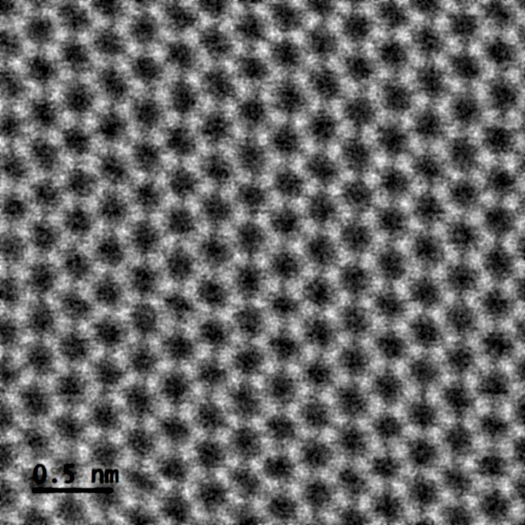
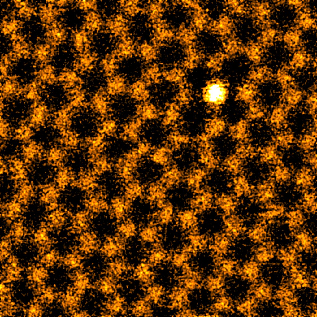
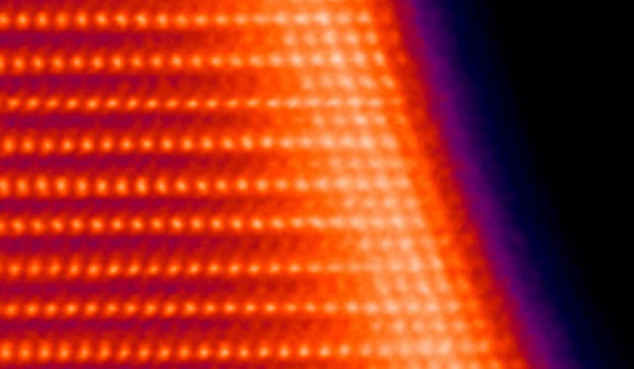
Some examples of standard ADF-STEM imaging are below:
ADF-STEM imaging of graphene and Si dopant in graphene at 80kV
ADF-STEM imaging of LiMnNiO2
