At UT-ACE, we aim to 1) create innovative circuits topologies and theories to address fundamental circuit challenges and enable new functionalities, 2) exploit synergies across the wireless system stack to break the limits in a conventionally partitioned design approach and advance the state of the art , and 3) leverage circuit techniques to meet the demanding performance requirements for various emerging applications. A few recent and ongoing research efforts are highlighted below.
RF/mmWave/THz Transceiver Front-End Circuits and Array Architectures
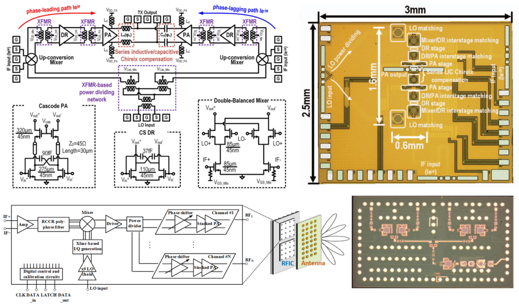
To address the exponentially growing data-rate demand, it is envisioned that high-frequency spectrum (e.g., mmWave) will be widely exploited in 5G-and-beyond wireless communication system for its broader available bandwidth and proportionate increase of channel capacity. To combat the deteriorated device performance and propagation conditions at high-frequencies, technological innovation at the circuit level is essential to break the convectional tradeoffs among different metrics (e.g., energy efficiency, linearity, bandwidth and noise) and satisfy the demanding performance requirements by future wireless network. To this end, we have been innovating both the fundamental building blocks in wireless transceivers and scalable array architectures to constantly push the achievable performance envelope.

Related Publications: ISSCC 2020 & JSSC 2020, SSC-L 2021, RFIC 2021.
Please explore our publications for more information.
AI-Driven RFIC Design Synthesis and Optimization
RFIC design has traditionally relied on intuition-driven methods, which have proven effective and have yielded a rich repertoire of design templates. However, as RF circuits and systems grow increasingly complex, conventional methodologies face challenges in balancing trade-offs between computational resource demands and performance optimization. The rapid advancements in artificial intelligence (AI) and machine learning (ML) present RFIC designers with a transformative opportunity to overcome these challenges. By leveraging these technologies, designers can break free from the labor-intensive cycle of iterative design and optimization, paving the way for more efficient and innovative design processes. We have been developing AI/ML-driven tools for RFIC design synthesis and optimization, aiming to significantly enhance productivity, lower entry barriers for beginners, and discover non-intuitive design topologies.

Related Publications: ICCAD 2024, ASPDAC 2025 & IMS 2025.
Please explore our publications for more information.
RF CMOS + “X” for GHz-to-THz Radios
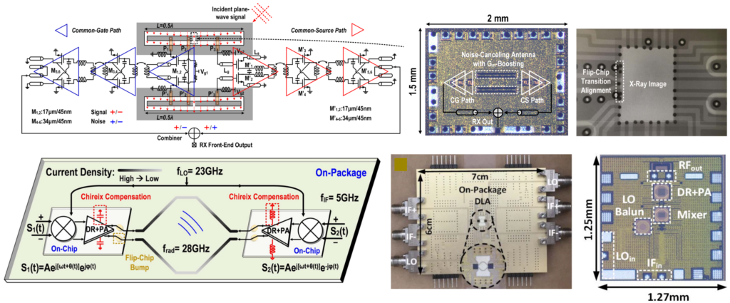
Conventionally, design of RF/wireless circuits and systems is partitioned into different levels of abstractions, i.e., devices, circuits, EM/antenna, etc. They are independent design spaces. Coupling is often undesirable and thus avoided, and a standardized interface is well defined to ease the system integration. However, such approach might lead to a locally optimized solution with limited design possibilities. As wireless is moving to a higher spectrum where the wavelength becomes comparable or even smaller than the device dimension, it is feasible and preferable to employ a holistic co-design methodology by further leveraging the versatile BEOL with unlimited/costless transistors in highly scaled silicon processes. As a result, the conventionally enforced boundary conditions are eliminated and new design spaces can be opened up, enabling new system architectures and performance breakthrough.

Related Publications: ISSCC 2020 & JSSC 2020, RFIC 2018 (best paper award) & JSSC 2019.
Please explore our publications for more information.
Antenna (Array), Passive Devices, and RF Packaging
As an integral part of wireless integrated circuits, passive devices sense and process signals at zero power consumption. Their reduced dimensions at mmWave and THz make it possible for on-chip implementations in which transistors can be used to precisely control the excitation and termination conditions across the passive structure. As a result, unique electromagnetic (EM) properties can be realized, such as reconfigurability, versatility, non-reciprocity, etc. In addition, the stringent requirements imposed by various emerging applications necessitate viable solutions to combine advantages from different technology platforms. Novel heterogeneous packaging techniques are thus investigated to address the challenges involving thermal and RF parasitic effect, and scalability.

Please explore our publications for more information.
