- eDRAM-CIM CNN Hardware Accelerator: In this work, a 1T1C eDRAM compute-in-memory engine is demonstrated in 65nm CMOS technology by repurposing 1T1C eDRAM columns as charge domain circuits to perform DNN computations. The key features are 1) support of in-eDRAM DNN analog computations: such as data conversion, dot-product, averaging, pooling, and rectified linear unit (ReLU) activation; (2) support for 8b input and 8b signed/unsigned weight multiply-accumulate-averaging (MAV) operations; (3) a modified WL controller to configure some of the 1T1C eDRAM columns as charge-sharing compute units in CIM mode; (4) performing dot products with non-destructive weight reads, thus avoiding weight duplication, extra control logic and not requiring a pre-initialized array; (5) an in-eDRAM adaptive dynamic-range successive-approximation (SAR) analog-to-digital converter (ADC) using narrow range of dot-product distribution to minimize the ADC latency/energy; and (6) quantify eDRAM- CIM benefits in an advanced eDRAM technology node. [ISSCC Paper] [ISSCC Slides]

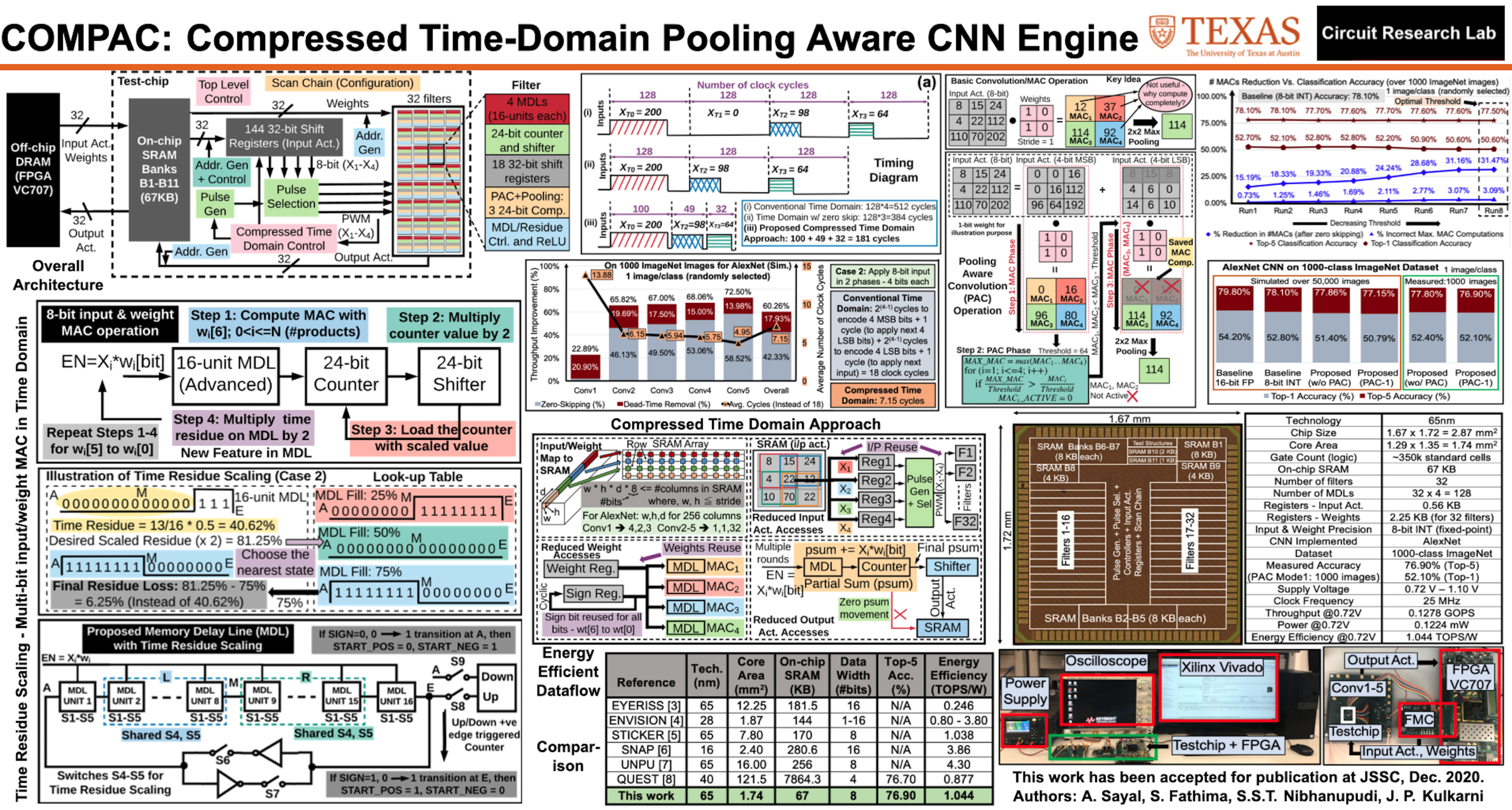
- COMPAC CNN Hardware Accelerator: In this work, a compressed time-domain, pooling aware convolution (COMPAC) CNN engine for an energy-efficient edge AI computing is demonstrated in 65nm CMOS technology. Four major ideas are proposed in this work which results in better performance, accuracy, and overall energy efficiency. The proposed COMPAC CNN engine supports time residue scaling (TRS) in the memory delay line (MDL) to perform an energy-efficient multi-bit input and weight MAC operation in the time-domain, while still achieving high classification accuracy. A compressed time-domain (CTD) approach is proposed and deployed in COMPAC to improve throughput in time encoding of the input activation. The simulation results on the AlexNet CNN over 1000 ImageNet images show a significant throughput improvement; consuming on an average, 14.71 and 7.15 input clock cycles to time encode an 8-bit input activation in two different compressed time-domain modes. Pooling Aware Convolution (PAC) technique is proposed to reduce the number of MACs. The simulation results on the AlexNet CNN over 1000 ImageNet images show up to 31.47% (21.79%) reduction in the number of non-zero input activations MACs with a top-5 classification accuracy loss of 0.60% (0.90%), top-1 classification accuracy loss of 2.20% (1.90%), and an on-chip access overhead of 60.53% (8.03%) for the PAC modes 1 (2) respectively. The trade-offs between classification accuracy, reduction in the number of MACs, and on-chip access need to be carefully comprehended to achieve optimal overall energy savings. An energy-efficient data flow for optimal on/off-chip memory accesses is also discussed in this paper. COMPAC data flow results in 86.97% reduced on-chip SRAM accesses and 29.74% reduced off-chip DRAM accesses compared to an Eyeriss, considering iso 8-bit precision. 65nm CMOS test-chip implementing the AlexNet CNN achieved an energy-efficiency of 1.044 TOPS/W, throughput of 0.1278 GOPS at 720mV while operating at 25MHz. The top-5 classification accuracy of 76.90% measured over 1000 ImageNet images, and 77.15% by simulating over 50,000 ImageNet images is achieved with the proposed COMPAC approach. The simulation results taken into account MDL circuit non-idealities over 50,000 ImageNet validation set images, show a classification accuracy loss within 1% when compared to the 8-bit fixed point software implementation.
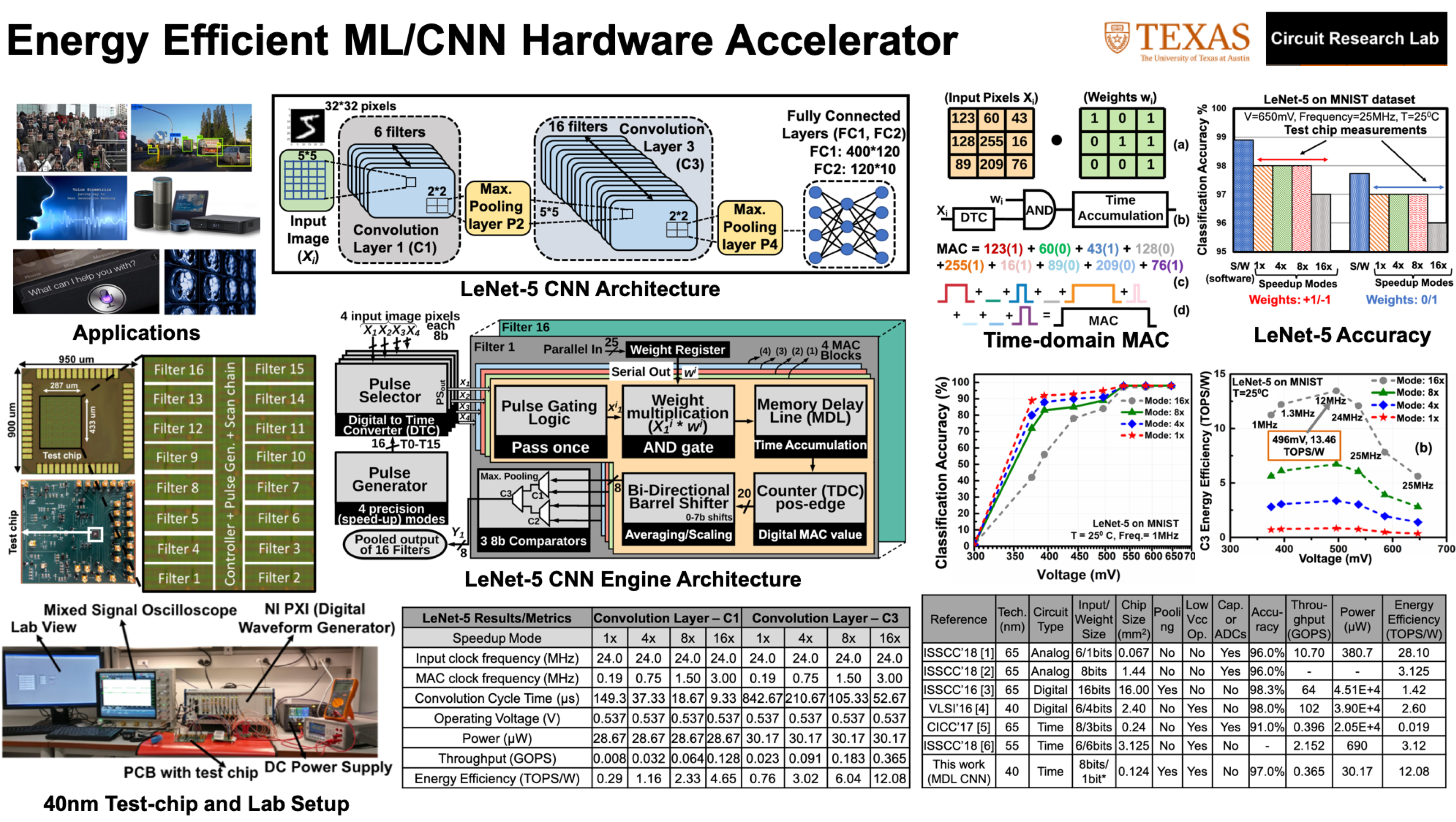
- ML/AI Hardware Accelerators: With the rapid progress in machine learning algorithms coupled with innovation in cloud compute resources; there has been unprecedented increase in the deployment of cognitive devices. However, cloud computation approach suffers from issues such as high latency, limited bandwidth, security and privacy concerns when transmitting data from edge to cloud. Thus, there is a need to develop energy efficient devices which run on battery to perform computation at edge. In this work, we propose and demonstrate an energy-efficient CNN engine for edge compute applications implemented in a 40nm CMOS featuring: 1) Bi-directional Memory Delay Lines (MDL) performing time-domain MAC operations; 2) multi-precision filter weight support (signed/unsigned 1-8b); 3) 16 filters each supporting 2×2 sub-sampling (max. pooling) and averaging; 4) all-digital, technology scalable design without requiring any capacitors, A/D converters, and/or frequency generators/modulators; and 5) near-threshold voltage operation supporting 16× speed-up with 4 input encoding modes. [ISSCC Paper] [JSSC Paper]
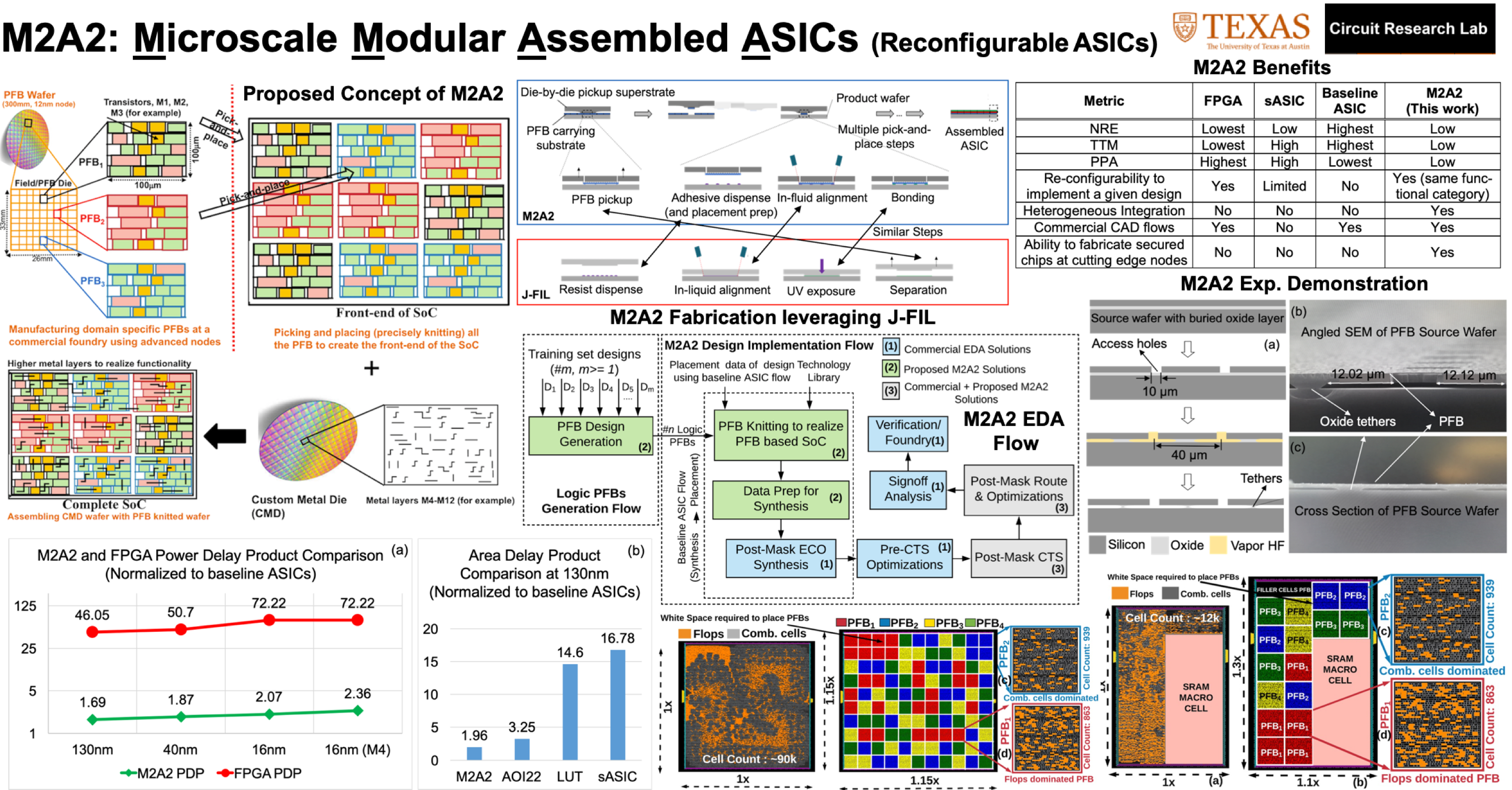
- Domain Specific Reconfigurable ASICs: With CMOS process technology scaling, the mask cost for fabricating nano-scale transistors, contacts and interconnects has become prohibitively expensive especially for low volume designs. Moreover, higher transistor density has resulted in higher design complexity and large-sized die, which has led to an increase in the design cycle time and degradation in the process yield. These challenges are forcing low-volume ASICs (Application Specific Integrated Circuits) towards highly sub-optimal FPGAs (Field Programmable Gate Arrays). In this work, we propose a new approach for designing and fabricating high- mix, low-volume heterogeneously integrated ASICs, referred to as Microscale Modular Assembled ASIC (M2A2), consisting of (1) pick-and-place assembly of pre-fabricated blocks (PFBs) which utilizes the nano-precision placement capabilities developed in Jet-and-Flash Imprint Lithography (J-FIL) and, (2) EDA design methodology utilizing unsupervised learning and graph-matching techniques. The EDA methodology leverages existing CAD tools infrastructure for easy adoption into the current EDA ecosystem. The proposed fabrication technology makes use of pick-and-place assembly techniques to allow nano-precise assembly of PFBs. The PFBs can be fabricated in advanced process nodes and then knitted together on a wafer substrate. Custom-designed low- cost back-end metal layers can then be created/placed on top of the PFB knitted layer to realize a variety of high-mix, low- volume ASIC designs. M2A2 would allow more flexibility in front- end design by optimal PFB selection and knitting compared to the earlier proposed approaches such as structured ASICs (sASICs). In this work, the performance of M2A2 based designs is compared with different design technologies such as baseline ASICs, FPGAs and sASICs at 16nm, 40nm and 130nm CMOS process nodes. The post-PNR simulation results achieved over 15 IWLS benchmarks show that the proposed M2A2 designs achieve 27.11x-34.89x reduced Power-Delay-Product (PDP) compared to FPGAs, and incur 1.69x-2.36x larger area compared to the baseline ASICs. The M2A2 designs achieve 15%-68.5% smaller area and 8.5%-52% higher performance compared to the sASIC methodologies. Moreover, the key fabrication steps in the proposed M2A2 technology are presented. The experimental fab results along with the proposed EDA flow simulations show promising results for the proposed M2A2 technology. Design trade-offs and process challenges for large scale deployment of the M2A2 technology are discussed along with their mitigation strategies. [TCAD Paper]
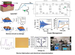
- Soft-FET:Voltage droops caused by the peak switching current as well sudden changes in current activity (di/dt) of various logic blocks results in IR drop as well as package inductance noise. This voltage droop attributes to a significant portion of the operating voltage specifications. In this research, we demonstrate energy efficient CMOS circuits using soft-switching transistors utilizing abrupt phase change in transition metal oxides (such as VO2). We propose a novel transistor architecture abbreviated as “Soft-FET”. By placing an optimized phase transition material in series with the gate terminal of a baseline MOSFET, its switching behavior can be smoothed out to reduce the peak current consumption, DAC 2018 [Paper].
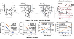
- NV-SRAM: Static Random-Access Memory (SRAM) technology is the enabler of advanced CMOS logic technology scaling and has significant implications on continuation of Moore’s law. Lower bitcell-leakage necessitates use of higher VT transistors which leads to higher active-Vmin (operating voltage). Therefore, there is a critical need to develop a unique SRAM technology which can decouple VT (for lower leakage) and active-Vmin constraints with zero area overheads. In this research we propose 6T-2R-2S (R= RRAM, S= Selector) SRAM bitcell featuring in-situ state retention, zero standby leakage, high density bitcell with no active area growth, decouple VT and Vmin design trade-off and heterogeneous integration of RRAM and selector devices using backend of the line (BEOL) process steps onto a baseline 6T SRAM CMOS design, VLSI-TSA 2019 [Paper].