“How can we fabricate something extremely small over large areas with high precision?” -Chih-Hao Chang
Nanostructures have received significant interest across many research disciplines for unique properties not found at the macro scale. As exciting as these advances may be, the transition from exploratory prototypes in a research setting to commercial products is a difficult engineering challenge. To address these challenges, we explore novel and unconventional nanofabrication techniques based on both “top-down” lithographic and “bottom-up” self-assembly approaches. Such a hybrid approach combines the advantages of both techniques.
3D Nanolithography using Colloidal Assembly
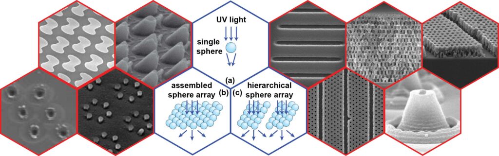
One process we are studying is using self-assembly of colloidal particles for near-field lithography to fabricate complex 3D structures [1]. In one approach, the nanosphere array is assembled into an hexagonal array directly on top of the substrate. The sphere array generates a 3D Talbot field when illuminated, which is then captured by the underlying photoresist. Light scattering from particles can also be utilized to generate interesting 3D nanostructures [2,3]. This approach replaces expensive optical components with self-assembled monolayer of nanospheres, allowing low-cost fabrication while maintaining pattern complexity as shown in the figure above [3].
Roll-to-Roll Printing of 3D Nanostructures

We are developing roll-to-roll 3D nanolithography based on particle-light interactions. In this approach, colloidal particles are illuminated with light as a near-field mechanism to pattern complex geometries. We have demonstrated patterning of 3D nanostructures on a 50×200 mm2 flexible substrate with a system throughput of 3 mm/s [4]. As with all manufacturing processes, metrology is essential in monitoring the precision and yield of the process. Using an automated electron beam inspection method, the prototype system has demonstrated high long-term repeatability and pattern uniformity of the system up to 85%.
Nanometrology

One important aspect of nanomanufacturing often overlooked is the precision of the fabricated structures. While some existing nanolithography approaches (such as electron beam, probed-based techniques, etc) may have high spatial resolution, their pattern placement accuracy over long distances can be magnitudes lower. Therefore nanometrology, or the measurement of nanoscale errors and defects, is critical. Using optical interferometric techniques, we were able to measure and correct for placement errors with high precision. In the above figure three and four sets of grating lines with 25 nm features were drawn in a serial process, demonstrating nanometer-level accuracy [5].
References
[1] C.-H. Chang, L. Tian, W. Hesse, H. Gao, H. J. Choi, M. Siddiqui, and G. Barbastathis, “From 2-dimensional self-assembly to 3-dimensional nanolithography,” Nano Letters, 2011, 11 (6), pp 2533–2537. [link]
[2] X. A. Zhang, J. Elek, and C.-H. Chang, “Three-Dimensional Nanolithography Using Light Scattering from Colloidal Particles,” ACS Nano, 7(7), 6212-6218, 2013. [link]
[3] X. A. Zhang, I-T. Chen and C.-H. Chang, “Recent progress in near-field nanolithography using light interactions with colloidal particles: from nanospheres to three-dimensional nanostructures,” 2019 Nanotechnology 30 352002 [link]
[4] I-T. Chen, E. Schappell, X. Zhang, and C.-H. Chang, “Continuous Roll-to-Roll Patterning of Three-Dimensional Periodic Nanostructures,” in press, Microsystems & Nanoengineering, January, 2020.
[5] C.-H. Chang, Y. Zhao, R. K. Heilmann, and M. L. Schattenburg, “Fabrication of 50 nm period gratings with multilevel interference lithography,” Optics Letters, 33, 1572-1574 (2008). [link]