Intel provides nice schematic diagrams of the layouts of their processor chips, but provides no guidance on how the user-visible core numbers and L3 slice numbers map to the locations on the die.
Most of the time there is no “need” to know the locations of the units, but there are many performance analyses that do require it, and it is often extremely helpful to be able to visualize the flow of data (and commands and acknowledgements) on the two-dimensional mesh.
In 2018 I spent a fair amount of time developing methodologies to determine the locations of the user-visible core and CHA/SF/LLC numbers on the Xeon Phi 7250 and Xeon Platinum 8160 processors. It required a fair amount of time because some tricks that Intel used to make it easier to design the photolithographic masks had the side effect of modifying the directions of up/down/left/right in different parts of the chip! When combined with the unknown locations of the disabled cores and CHAs, this was quite perplexing….
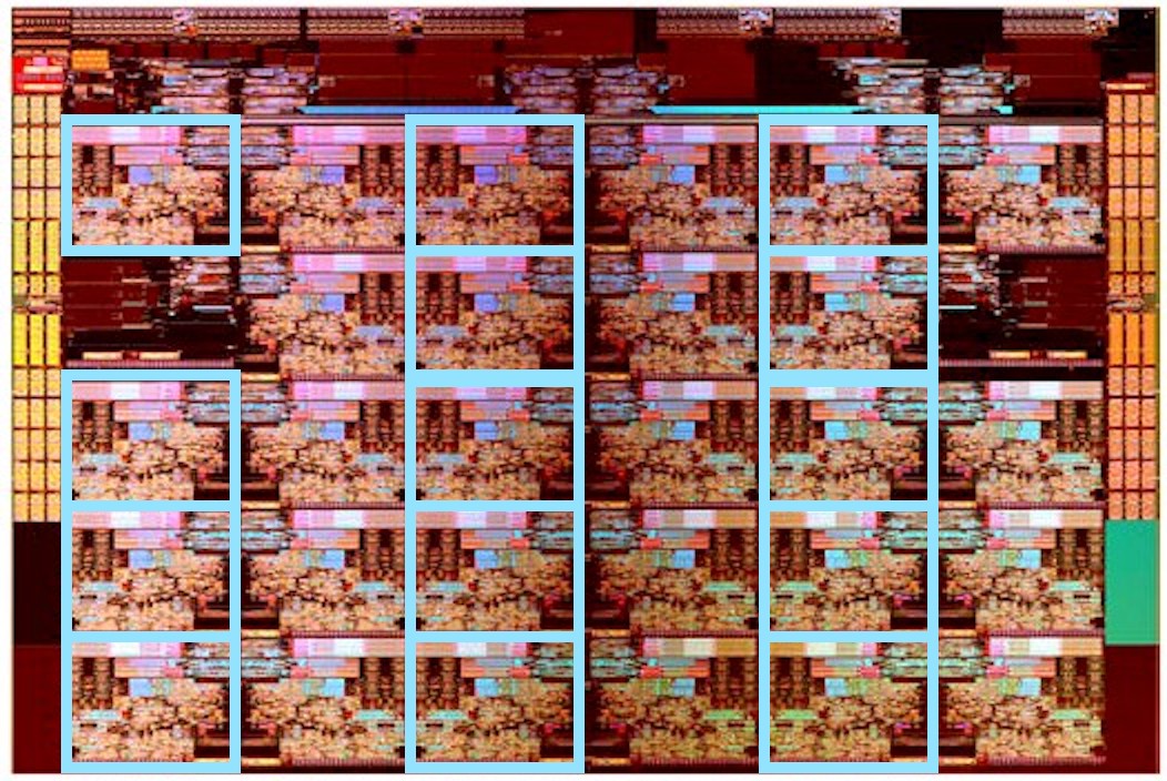
The Xeon Scalable Processors (Skylake, Cascade Lake, and the new Ice Lake Xeon) “mirror” the photolithographic mask for the “Tile” (Core + CHA/SF/LLC) in alternating columns, causing the meanings of “left” and “right” in the mesh traffic performance counters to alternate as well. This is vaguely hinted by some of the block diagrams of the chip (such as XeonScalableFamilyTechnicalOverviewFigure5, but is more clear in the die photo:

Here I have added light blue boxes around the 14 (of 28) Tile locations on the die that have the normal meanings of “left” and “right” in the mesh data traffic counters. The Tiles that don’t have blue boxes around them are left-right mirror images of the “normal” cores, and at these locations the mesh data traffic counters report mesh traffic with “left” and “right” reversed. NOTE that the 3rd Generation Intel Xeon Scalable Processors (Ice Lake Xeon) show the same column-by-column reversal as the Skylake Xeon, leading to the same behavior in the mesh data traffic counters.
TACC Frontera System
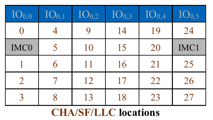
For the Xeon Platinum 8280 processors in the TACC Frontera system, all 28 of the Tiles are fully enabled, so there are no disabled units at unknown locations to cause the layout and numbering to differ from socket to socket. In each socket, the CHA/SF/LLC blocks are numbered top-to-bottom, left-to-right, skipping over the memory controllers:

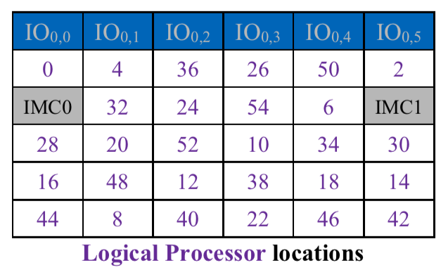
The pattern of Logical Processor numbers will vary depending on whether the numbers alternate between sockets (even in 0, odd in 1) or are block-distributed (first half in 0, second half in 1). For the TACC Frontera system, all of the nodes are configured with logical processors alternating between sockets, so all even-numbered logical processors are in socket 0 and all odd-numbered logical processors are in socket 1. For this configuration, the locations of the Logical Processor numbers in socket 0 are:

In socket 1 the layout is the same, but with each Logical Processor number incremented by 1.
More details are in TR-2021-01b (link below in the references).
TACC Stampede2 System
“Skylake Xeon” partitions
For the Xeon Platinum 8160 processors in the TACC Stampede2 system, 24 of the Tiles are fully enabled and the remaining 4 Tiles have disabled Cores and disabled CHA/SF/LLCs. For these processors, administrative privileges are required to read the configuration registers that allow one to determine the locations of the CHA/SF/LLC units and the Logical Processors. There are approximately 120 different patterns of disabled tiles across the 3472 Xeon Platinum 8160 processors (1736 2-socket nodes) in the Stampede2 “SKX” partitions. The pattern of disabled cores generally has negligible impact on performance, but one needs to know the locations of the cores and CHA/SF/LLC blocks to make any sense of the traffic on the 2D mesh. Fortunately only one piece of information is needed on these systems — the CAPID6 register tells which CHA locations on the die are enabled, and these systems have a fixed mapping of Logical Processor numbers to co-located CHA numbers — so it would not be hard to make this information available to interested users (if any exist).
More details are in TR-2021-01b (link below in the references).
“Knights Landing” (“KNL”) partitions
For the 4200 Stampede2 nodes with Xeon Phi 7250 processors, all 38 CHA/SF units are active in each chip, and 34 of the 38 tiles have an active pair of cores. Since all 38 CHAs are active, their locations are the same from node to node:
For these processors the information required to determine the locations of the cores is available from user space (i.e., without special privileges). The easiest way to do this is to simply use the “/proc/cpuinfo” device to get the “core id” field for each “processor” field. Since each core supports four threads, each of the “core id” fields should appear four times. Each tile has two cores, so we take the even-numbered “core id” fields and divide them by two to get the tile number where each of the active cores is located. A specific example showing the Logical Processor number, the “core id”, and the corresponding “tile” location:
c455-003.stampede2:~/Stampede2/Configurations:2021-05-27T12:39:28 $ grep ^processor /proc/cpuinfo  | head -68 | awk '{print $NF}' > tbl.procs
c455-003.stampede2:~/Stampede2/Configurations:2021-05-27T12:39:55 $ grep "^core id" /proc/cpuinfo  | head -68 | awk '{print $NF}' > tbl.coreids
c455-003.stampede2:~/Stampede2/Configurations:2021-05-27T12:40:22 $ grep "^core id" /proc/cpuinfo  | head -68 | awk '{print int($NF/2)}' > tbl.tiles
c455-003.stampede2:~/Stampede2/Configurations:2021-05-27T12:40:32 $ paste tbl.procs tbl.coreids tbl.tiles
0	0	0
1	1	0
2	2	1
3	3	1
4	4	2
5	5	2
6	6	3
7	7	3
8	8	4
9	9	4
10	10	5
11	11	5
12	12	6
13	13	6
14	14	7
15	15	7
16	16	8
17	17	8
18	18	9
19	19	9
20	22	11
21	23	11
22	24	12
23	25	12
24	26	13
25	27	13
26	28	14
27	29	14
28	30	15
29	31	15
30	32	16
31	33	16
32	34	17
33	35	17
34	36	18
35	37	18
36	38	19
37	39	19
38	40	20
39	41	20
40	42	21
41	43	21
42	44	22
43	45	22
44	46	23
45	47	23
46	48	24
47	49	24
48	50	25
49	51	25
50	56	28
51	57	28
52	58	29
53	59	29
54	60	30
55	61	30
56	62	31
57	63	31
58	64	32
59	65	32
60	66	33
61	67	33
62	68	34
63	69	34
64	70	35
65	71	35
66	72	36
67	73	36
For each Logical Processor (column 1), the tile number is in column 3, and the location of the tile is in the figure above.
Since the tile numbers are [0..37], from this list we see that 10, 26, 27, and 37 are missing, so these are the tiles with disabled cores.
More details are in TR-2020-01 and in TR-2021-02 (links below in the references).
Presentations:
- Topology and Cache Coherence in Knights Landing and Skylake Xeon Processors
- Address Hashing in Intel Processors
Detailed References:
- Observations on Core Numbering and Core ID’s in Intel Processors (Technical Report TR-2020-01)
- Mapping Core and L3 Slice Numbering to Die Location in Intel Xeon Scalable Processors (Technical Report TR-2021-01b)
- Mapping Core, CHA, and Memory Controller Numbers to Die Locations in Intel Xeon Phi x200 (“Knights Landing”,”KNL”) Processors (Technical Report TR-2021-02)
What is a CHA/SF/LLC ? This is a portion of each Tile containing a “Coherence and Home Agent” slice, a “Snoop Filter” slice, and a “Last Level Cache” slice. Each physical address in the system is mapped to exactly one of the CHA/SF/LLC blocks for cache coherence and last-level caching, so that (1) any core in the system will automatically make use of all of the LLC slices, and (2) each CHA/SF/LLC has to handle approximately equal amounts of work when all the cores are active.

