
– Raw data, experimental set-up details, fabrication procedures, etc. available upon reasonable request.
2026
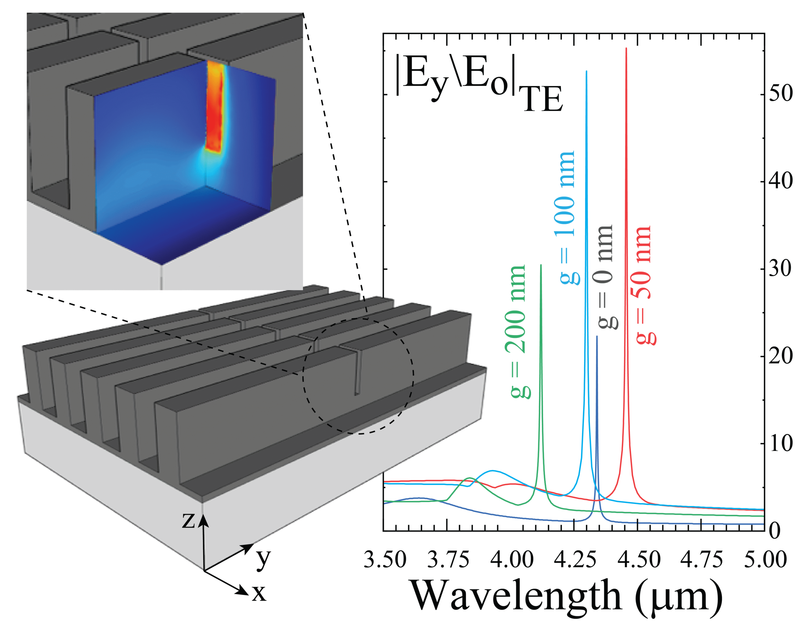
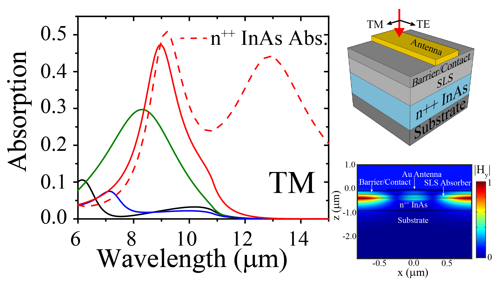
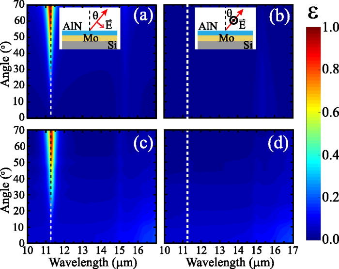
168. “Asymmetry-Enabled Dual-Resonant Mid-Infrared Absorption in Subwavelength Perforated Metal Structures“, Silvia Guadagnini, Shadman Shahid, Zarko Sakotic, Divya Hungund, Daniel Wasserman, and Michelle L. Povinelli, Nano Letters (2026)

167. “Room-Temperature Mid-Wave Infrared Guided Mode Resonance Photodetectors for Focal Plane Arrays“, N.C. Mansfield, M. Bergthold, Y. Tischenko, S. Purkait, Y. Magendzo Behar, E. Chow, Edmond and A. Francis, V.A. Podolskiy, and D. Wasserman, IEEE Journal of Selected Topics in Quantum Electronics, 32(3), 3800509 (2026).
166. “Mid-Infrared Metaplasmonic Sensing”, Divya Hungund, Noah Mansfield, Jeffery Allen, Monica Allen, Zarko Sakotic, and Daniel Wasserman, Nano Letters (2026).

165. “Dynamic Control of Polarization States with Barium Titanate Integrated Photonic Devices”, D. Krueger, L. Tian, D. Hungund, H.G. Kim, A. Raju, A. Posadas, A.A. Demkov, and D. Wasserman, Appl. Phys. Lett., 128, 161106 (2026).

164. “Thermo-Optic Control of Barium Titanate Modulators on Silicon-on-Insulator Substrates“, Hee Gon Kim, A. Raju, L. Tian, D. Krueger, A. Posadas, A. A. Demkov, and D. Wasserman, IEEE Photonics Technology Letters, 38, 819 (2026).
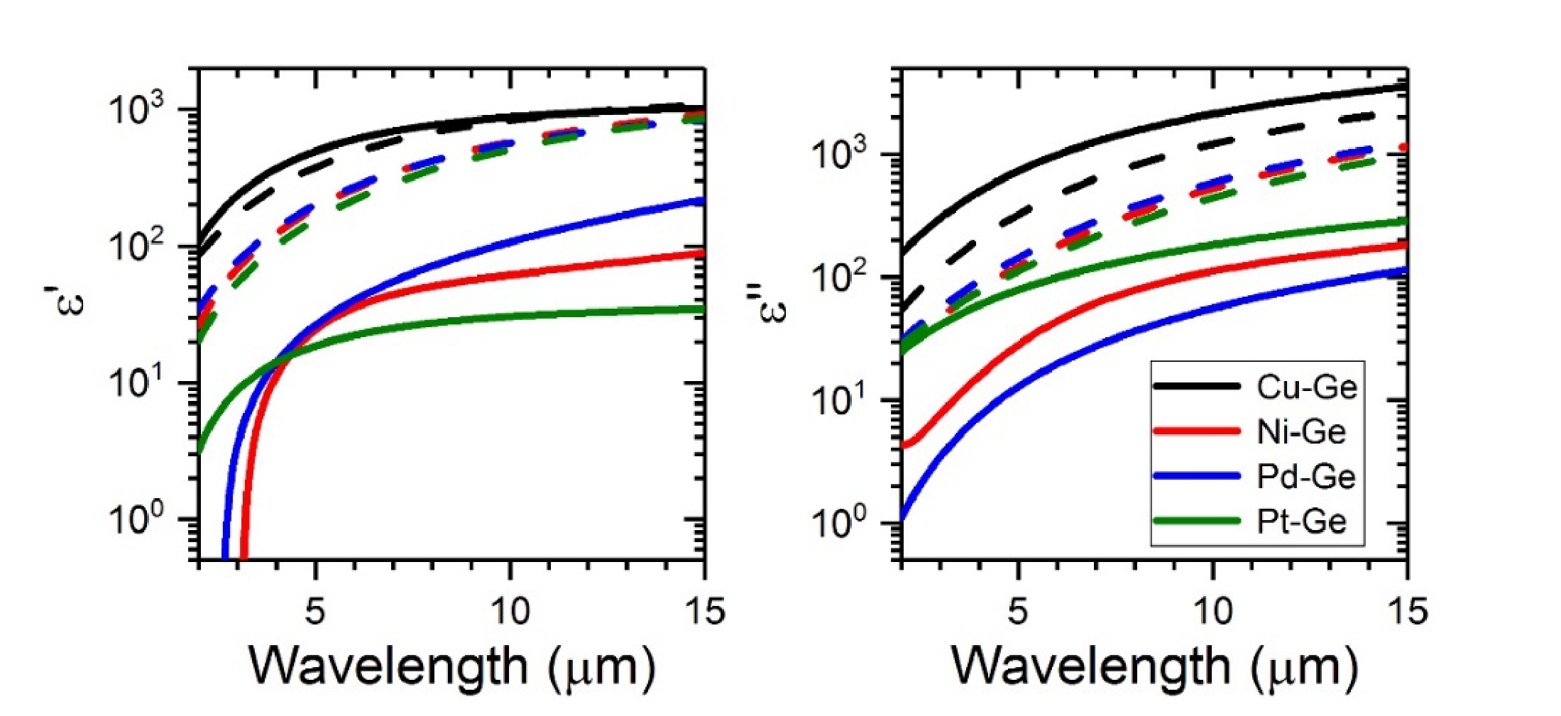
163. “Dilute noble metal films for infrared optics and plasmonics [Invited]“, Zarko Sakotic, Noah C. Mansfield, and Daniel Wasserman, Opt. Mater. Express 16, 1001-1014 (2026).
Pioneers in Optical Materials Feature Issue

162. “Epitaxial Materials for Photonics: feature issue introduction“, Leland Nordin, Sadhvikas Addamane, David Lackner, Shubhra Pasayat, Fumitaro Ishikawa, and Daniel Wasserman, Opt. Mater. Express, 16, 824-829 (2026)
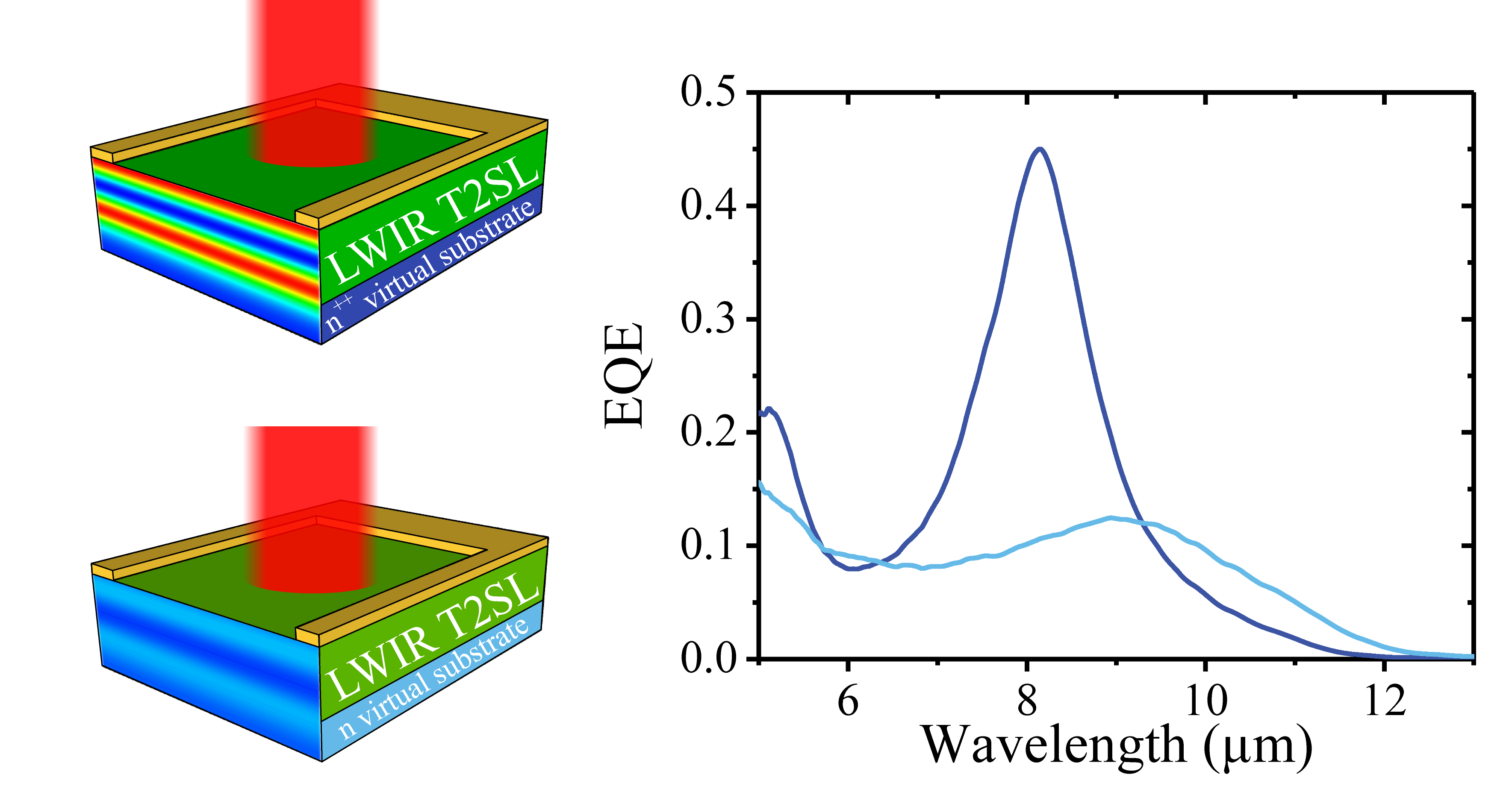
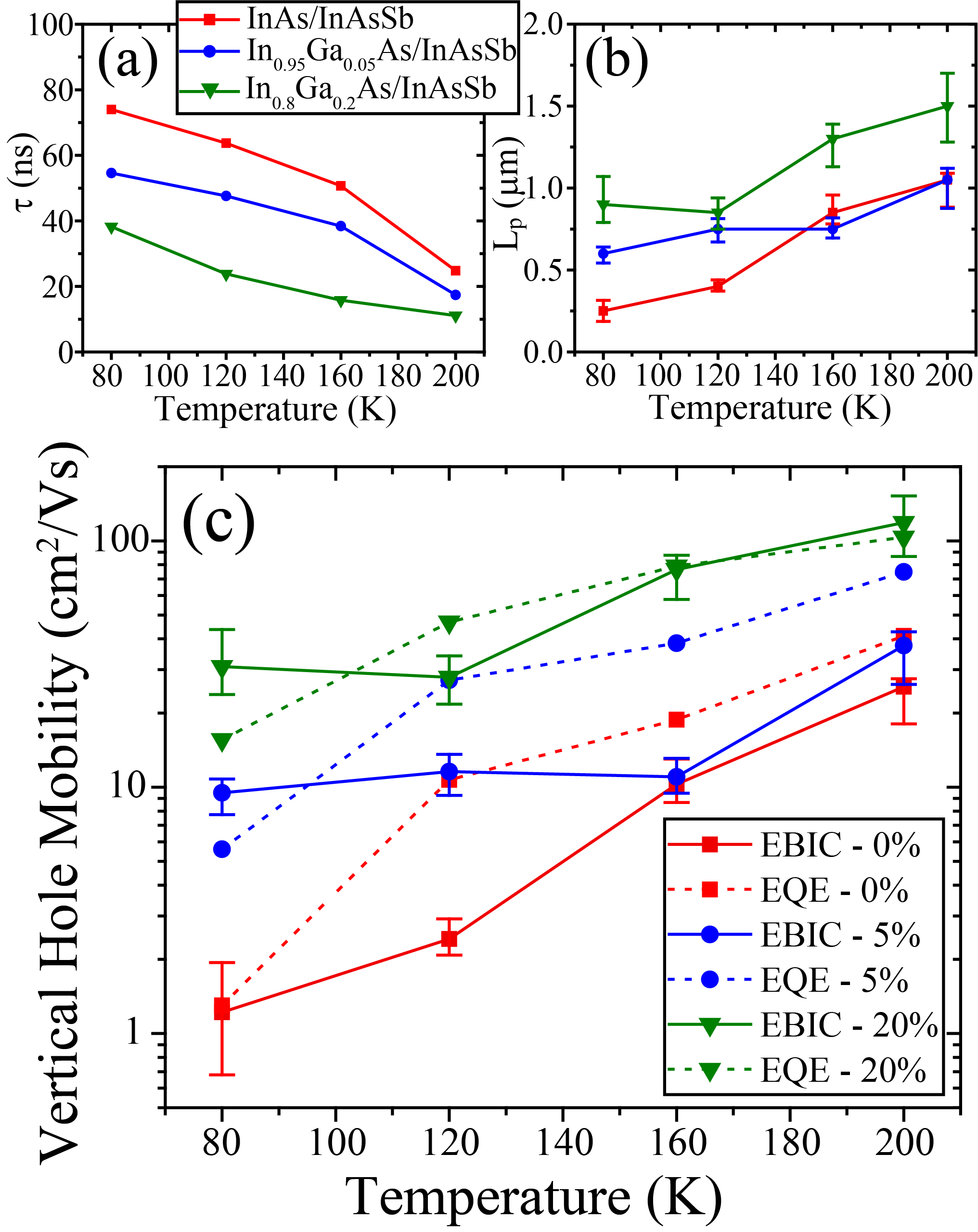
161. “Extended wavelength dilute-bismide infrared nBn photodetectors on InSb“, R. C. WhiteM. K. BergtholdF. A. Estévez HA. F. RicksD. WassermanS. R. Bank, Appl. Phys. Lett., 128, 072102 (2026).
160. “Subdiffractive confinement of ultrashort mid-IR pulses with photonic funnels“, J. LaMountain, A. Raju, D. Wasserman, and V. A. Podolskiy, Opt. Express 34(4), 6858-6869 (2026).

2025
159. “Self-assembled mid-infrared metasurfaces for high-contrast femtosecond switching”, Zarko Sakotic, Madeline Brown, Woo Je Chang, Lauralee E. Hurst, Noah Mansfield, Tanay Paul, Thomas M. Truskett, Monica Allen, Jeffery Allen, Delia J. Milliron, Daniel Wasserman, Advanced Photonics, 8, 026001 (2026).
158. “Guided mode slot resonators “, Noah C. Mansfield, Alexander Ware, Amogh Raju, Divya Hungund, Zuoming Dong, Yonathan Magendzo Behar, William J. Doyle, Edmond Chow, Anitta Francis, Monica Allen, Jeffery Allen, Zarko Sakotic, and Daniel Wasserman, Applied Physics Letters, 127, 181103 (2025)

Crystal Growth & Design (2025)
150. “Infrared Metaplasmonics”, Zarko Sakotic, Noah Mansfeld, Amogh Raju, Alexander Ware, Divya Hungund, Daniel Krueger, Daniel Wasserman, ACS Photonics (2025).
149. “Ultrastrong Coupling by Assembling Plasmonic Metal Oxide Nanocrystals in Open Cavities”, W.J. Chang, B. Roman, T. Paul, Z. Sakotic, P. Vora, K. Kim, D. Wasserman, T. Truskett, D. Milliron, ACS Nano, 19 12332 (2025).
2024
148. “Plasmonic Metal Oxide Nanocrystals as Building Blocks for Infrared Metasurfaces“,
Woo Je Chang, Allison M. Green, Zarko Sakotic, Daniel Wasserman, Thomas M. Truskett, and Delia J. Milliron, Accounts of Materials Research, 6, 104–113 (2025)

147. “Observation of low-resistance Al and Ni p-type ohmic contacts to dilute GeC and GeCSn alloys“, J.K. Saha, S. A. A. Taqy, P. K. Sarkar, I. Rahaman, A. W. Arbogast, T. Dey, A. Dolocan, Md. Reaz Rahman Munna, K. Alam, D. Wasserman, S. R. Bank, M. A. Wistey, J. Vac. Sci. Technol. B 42, 062211 (2024)
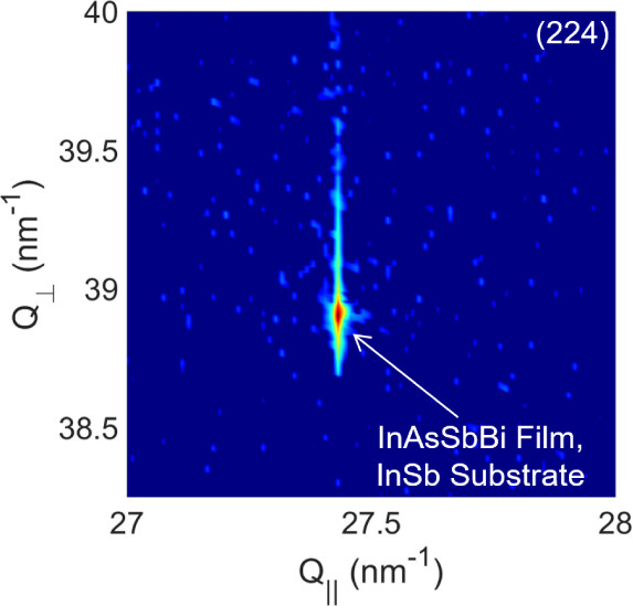
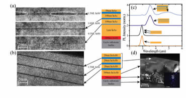
146. “Molecular Beam Epitaxy of InAsSbBi Lattice-Matched to InSb toward Long-Wave Infrared Sensing“, R. Corey White, Morgan Bergthold, Aaron Muhowski, Leland Nordin, Iris Okoro, Hussein Hijazi, Leonard Feldman, Daniel Wasserman, and Seth R. Bank, Crystal Design and Growth (2024)
145. “Room temperature mid-wave infrared guided mode resonance InAsSb photodetectors“, N. C. Mansfield, Y. Tischenko, M. Bergthold, S. Purkait; A. Raju; A. Kamboj, V. A. Podolskiy, and D. Wasserman, Applied Physics Letters (Special Collection: Mid and Long Wavelength Infrared Photonics, Materials, and Devices), 125, 171107 (2024).
144. “Anomalous reflection for highly efficient subwavelength light concentration and extraction with photonic funnels”, J. LaMountain, A. Raju, D. Wasserman, and V.A. Podolskiy, Nanophotonics, 2024.
143. “Mid-Infrared Perfect Absorption with Planar and Subwavelength-Perforated Ultrathin Metal Films“, Zarko Sakotic, Amogh Raju, Alexander Ware, Félix A. Estévez H., Madeline Brown, Yonathan Magendzo Behar, Divya Hungund, Daniel Wasserman, Advanced Physics Research, 3, 2400012 (2024)
142. “Structural Order and Plasmonic Response of Nanoparticle Monolayers“, Allison M. Green, Woo Je Chang, Zachary M. Sherman, Zarko Sakotic, Kihoon Kim, Daniel Wasserman, Delia J. Milliron, and Thomas M. Truskett, ACS Photonics (2024)

141. Featured Article: “High-Speed Long-Wave Infrared Ultra-Thin Photodetectors”, Yinan Wang, Aaron J. Muhowski, Leland Nordin, Sukrith Dev, Monica Allen, Jeffery Allen, Daniel Wasserman, APL Photonics, 9, 016117 (2024).
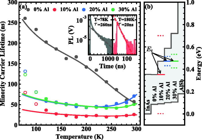
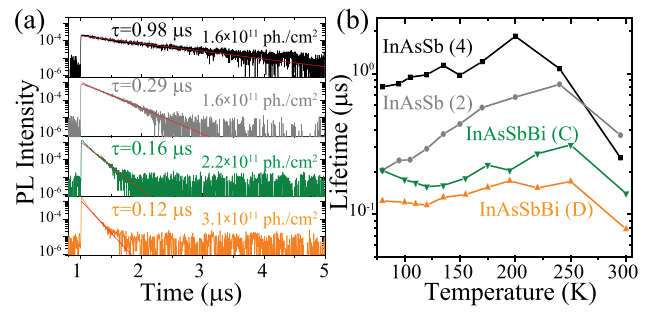
140. “Enhanced minority carrier lifetime in bulk hydrogen-passivated InAsSbBi”, Félix A. Estévez H., M. Bergthold, Oleg Maksimov, Harish B. Bhandari, Christian P. Morath, Alexander W. Duchane, Preston T. Webster, and D. Wasserman, Applied Physics Letters, 124, 021104 (2024).
2023
138. “Monolithic Barium Titanate Modulators on Silicon-on-Insulator Substrates”, Zuoming Dong, Amogh Raju, Agham B. Posadas, Marc Reynaud, Alexander A. Demkov, and Daniel M. Wasserman, ACS Photonics, 10, 4367–4376 (2023)
137. “Influence of H on Sn incorporation in GeSnC alloys grown using molecular beam epitaxy“, Tuhin DeyAugustus W. ArbogastQian MengMd. Shamim RezaAaron J. MuhowskiJoshua J. P. CooperErdem OzdemirFabian U. NaabThales BorrelyJonathan AndersonRachel S. GoldmanDaniel WassermanSeth R. BankMark W. HoltzEdwin L. PinerMark A. Wistey, J. Appl. Phys., 134, 193102 (2023).
136. “Growth of tin-free germanium carbon alloys using carbon tetrabromide (CBr4)“, Md. Shamim RezaTuhin DeyAugustus W. ArbogastAaron J. MuhowskiMark W. HoltzChad A. StephensonSeth R. BankDaniel WassermanMark A. Wistey; J. Appl. Phys., 134, 183103 (2023).

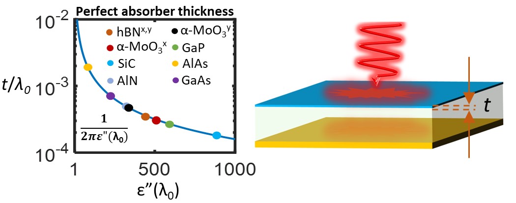
135. “Perfect Absorption at the Ultimate Thickness Limit in Planar Films“, Zarko Sakotic, Alexander Ware, Michelle Povinelli, and Daniel Wasserman, ACS Photonics, 10, 4244 (2023).
134. “Decoupling absorption and radiative cooling in mid-wave infrared bolometric elements” Alexander Ware, Morgan Bergthold, Noah Mansfield, Zarko Sakotic, Ethan A. Scott, C. Thomas Harris, and Daniel Wasserman, Optics Letters, 48, 3155-3158 (2023).
133. “Quantum dot materials for mid-IR photodetection: opinion“, Haemin Song, Yadviga Tischenko, Daniel Wasserman, and Kwang Seob Jeong, Optical Materials Express, 13, 1328 (2023).
132. “Response times of a degenerately doped semiconductor based plasmonic modulator“, Raj K. Vinnakota, Zuoming Dong, Andrew F. Briggs, Seth R. Bank, Daniel Wasserman, and Dentcho A. Genov, J. Optical Society of America B, 40, 978 (2023).

131. “Low-threshold visible InP quantum dot and InGaP quantum well lasers grown by molecular beam epitaxy“, Pankul Dhingra, Aaron J. Muhowski, Brian D. Li, Yukun Sun, Ryan D. Hool, Daniel Wasserman, and Minjoo Larry Lee, J. Appl. Phys. 133, 103101 (2023).

130. “High-speed mid-wave infrared holey photodetectors“, Yinan Wang, Leland Nordin, Sukrith Dev, Monica Allen, Jeffery Allen, and Daniel Wasserman, Journal of Applied Physics 133, 104501 (2023);
129. “High-gain low-excess-noise MWIR detection with a 3.5-μm cutoff AlInAsSb-based separate absorption, charge, and multiplication avalanche photodiode“, Adam A Dadey, J. Andrew McArthur, Abhilasha Kamboj, Seth R. Bank, Daniel Wasserman and Joe C. Campbell, APL Photonics 8, 036101 (2023);
2022


119. “High operating temperature plasmonic infrared detectors“, Leland Nordin, Aaron J. Muhowski, and Daniel Wasserman, Applied Physics Letters, 120, 101103 (2022).
118. “Extending plasmonic response to the mid-wave infrared with all-epitaxial composites“, Aaron J. Muhowski, Evan Simmons, Kun Li, Evgenii E. Narimanov, Viktor A. Podolskiy, and Daniel Wasserman, Opt. Lett. 47(4), 973-976 (2022).
117. “Cascaded InGaSb quantum dot LEDs“, A. J. Muhowski, A. Kamboj, A.F. Briggs, L. Nordin, S. R. Bank, and D. Wasserman, J. Appl. Phys. 131, 043105 (2022).

2021
116. “Minority carrier lifetimes in digitally-grown, narrow-gap, AlInAsSb alloys“, A. J. Muhowski, S. D. March, S. J. Maddox, D. Wasserman, and S. R. Bank, Appl. Phys. Lett. 119, 251102 (2021).
115. “Ultra-thin plasmonic detectors“, Leland Nordin, Priyanka Petluru, Abhilasha Kamboj, Aaron J. Muhowski, and Daniel Wasserman, Optica, 8, 1545 (2021).

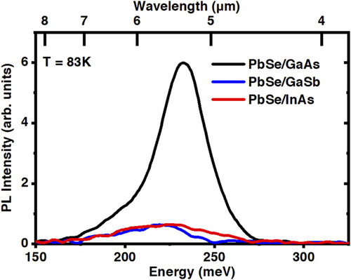
114. “Bright mid-infrared photoluminescence from high dislocation density epitaxial PbSe films on GaAs“, Jarod Meyer, Aaron J. Muhowski, Leland Nordin, Eamonn Hughes, Brian Haidet, Daniel Wasserman, and Kunal Mukherjee, APL Materials 9, 111112 (2021).
113. “Low-threshold InP quantum dot and InGaP quantum well visible lasers on silicon (001)“, Pankul Dhingra, Patrick Su, Brian D. Li, Ryan D. Hool, Aaron J. Muhowski, Mijung Kim, Daniel Wasserman, John Dallesasse, and Minjoo Larry Lee, Optica, 8, 2334 (2021).

112. “Measuring Molecular Diffusion Through Thin Polymer Films with Dual-Band Plasmonic Antennas“, Hao Chen, Gaurav Singhal, Frank Neubrech, Runyu Liu, Joshua S. Katz, Scott Matteucci, Steven G. Arturo, Daniel Wasserman, Harald Giessen, and Paul V. Braun, ACS Nano (2021).

111. “All-epitaxial guided-mode resonance mid-wave infrared detectors”, A. Kamboj, L. Nordin, P. Petluru, A. J. Muhowski, D. N. Woolf, and D. Wasserman, Appl. Phys. Lett. 118, 201102 (2021).
110. “All-epitaxial long-range surface plasmon polariton structures with integrated active materials“, L. Nordin*, P. Petluru*, A.J. Muhowski, E.A. Shaner, and Daniel Wasserman, J. Appl. Phys., 129, 113102 (2021).
*Authors contributed equally
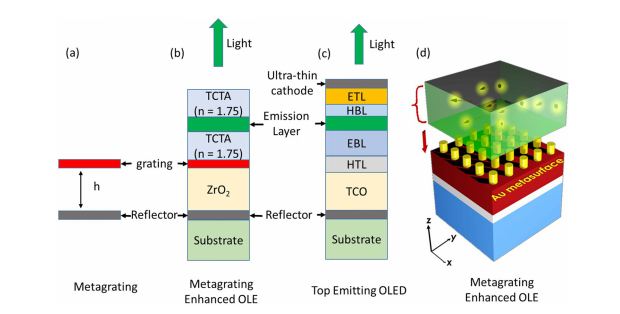
109. “Reflecting Metagrating-Enhanced Thin-Film Organic Light Emitting Devices“, Xin Xu, Hoyeong Kwon, Stanley Finch, Jae Young Lee, Leland Nordin, Daniel Wasserman, Andrea Alù, and Ananth Dodabalapur, Appl. Phys. Lett., 118, 053302 (2021).
108. “Interface structure and luminescence properties of epitaxial PbSe films on InAs(111)A“, Brian B. Haidet, Leland Nordin, Aaron J. Muhowski, Kevin D. Vallejo, Eamonn T. Hughes, Jarod Meyer, Paul J. Simmonds, Daniel Wasserman, and Kunal Mukherjee, J. Vac. Sci. Technol. A, 39, 023404 (2021).
2020
107. “Ballistic Metamaterials“, Kun Li, Evan Simmons, Andrew F. Briggs, Seth R. Bank, Daniel Wasserman, Viktor A. Podolskiy, and Evgenii E. Narimanov, Optica, 7, 1773-1780 (2020).

106. “Subdiffraction Limited Photonic Funneling of Light“, K. Li, E. Simmons, A.F. Briggs, L. Nordin, J. Xu, V. Podolskiy and D. Wasserman, Advanced Optical Materials, 2001321 (2020)
105. “Enhanced room temperature infrared LEDs using monolithically integrated plasmonic materials“, A.F. Briggs, L. Nordin, A.J. Muhowski, E. Simmons, P. Dhingra, M.L. Lee, V.A. Podolskiy, D. Wasserman, and S.R. Bank, Optica 7, 1355-1358 (2020)
104. “Engineering the Berreman mode in mid-infrared polar materials“, Irfan Khan, Zhaoyuan Fang, Milan Palei, Junchi Lu, Leland Nordin, Evan L. Simmons, Owen Dominguez, S. M. Islam, Huili Grace Xing, Debdeep Jena, Viktor A. Podolskiy, Daniel Wasserman, and Anthony J. Hoffman, Optics Express, 28, 28590 (2020).
103. “Minority carrier lifetime and photoluminescence of mid-wave infrared InAsSbBi“, Priyanka Petluru, Perry C. Grant, Aaron J. Muhowski, Isabella M. Obermeier, Marko S. Milosavljevic, Shane R. Johnson, Daniel Wasserman, Elizabeth H. Steenbergen, and Preston T. Webster, Appl. Phys. Lett., 117, 061103 (2020). https://doi.org/10.1063/5.0007275
102. “All-Epitaxial Integration of Long-wavelength Infrared Plasmonic Materials and Detectors for Enhanced Responsivity“, Leland Nordin, Abhilasha Kamboj, Priyanka Petluru, Eric Shaner, and Daniel Wasserman, ACS Photonics 7, 1950–1956 (2020). https://doi.org/10.1021/acsphotonics.0c00659
101. “Insb Pixel-Loaded InSb pixel loaded microwave resonator for high-speed mid-wave infrared detection”
Y. Wang, S. Dev, F. Yang, L. Nordin, Y. Wang, A. Briggs, M. Allen, J. Allen, E. Tutuc, and D. Wasserman, Infr. Phys. Tech., 109, 103390 (2020).
100. “Plasmonic electro-optic modulator based on degenerate semiconductor interfaces“, R.K. Vinnakota, Z. Dong, A.F. Briggs, S.R. Bank, D. Wasserman, and D.A. Genov, Nanophotonics (2020)

99. “Room Temperature Mid Infrared Detection via Resonant Microwave Circuits“, Sukrith Dev, Yinan Wang, Yimeng Wang, Monica Allen, Jeffery Allen, Emanuel Tutuc, and Daniel Wasserman, IEEE Trans. Electron. Dev., 67(4), 1632-1638, (2020)

98. “Mid-infrared electroluminescence from type-II In(Ga)Sb quantum dots“, Andrew F. Briggs, Leland J. Nordin, Aaron J. Muhowski, Priyanka Petluru, David Silva, Daniel Wasserman, and Seth R. Bank, Appl. Phys. Lett., 116, 061103 (2020).

97. “Enhanced emission from ultra-thin long wavelength infrared superlattices on epitaxial plasmonic materials“, L. Nordin, K. Li, A. Briggs, E. Simmons, S. R. Bank, V. A. Podolskiy, and D. Wasserman, Appl. Phys. Lett., 116, 021102 (2020)
2019
96. “Phonon-polaritonics: enabling powerful capabilities for infrared photonics“, Stavroula Foteinopoulou, Ganga Chinna Rao Devarapu, Ganapathi S. Subramania, Sanjay Krishna, and Daniel Wasserman, Nanophotonics, 8(12) 2129-2175 (2019)
95. News and Views: “Nanosecond modulation of thermal emission“, Daniel Wasserman , Light: Science & Applications, 8, 68 (2019).
94. “Electrical modulation of degenerate semiconductor plasmonic interfaces“, Z. Dong, R.K. Vinnakota, A.F. Briggs, L. Nordin, S.R. Bank, D.A. Genov, and D. Wasserman, J. Appl. Phys., 126, 043101 (2019).
93. “Probing polaritons in the mid- to far-infrared“, T.G. Folland, L. Nordin, D. Wasserman, and J.D. Caldwell, Journal of Applied Physics 125, 191102 (2019) Featured
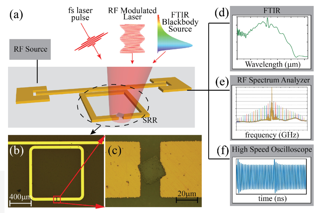
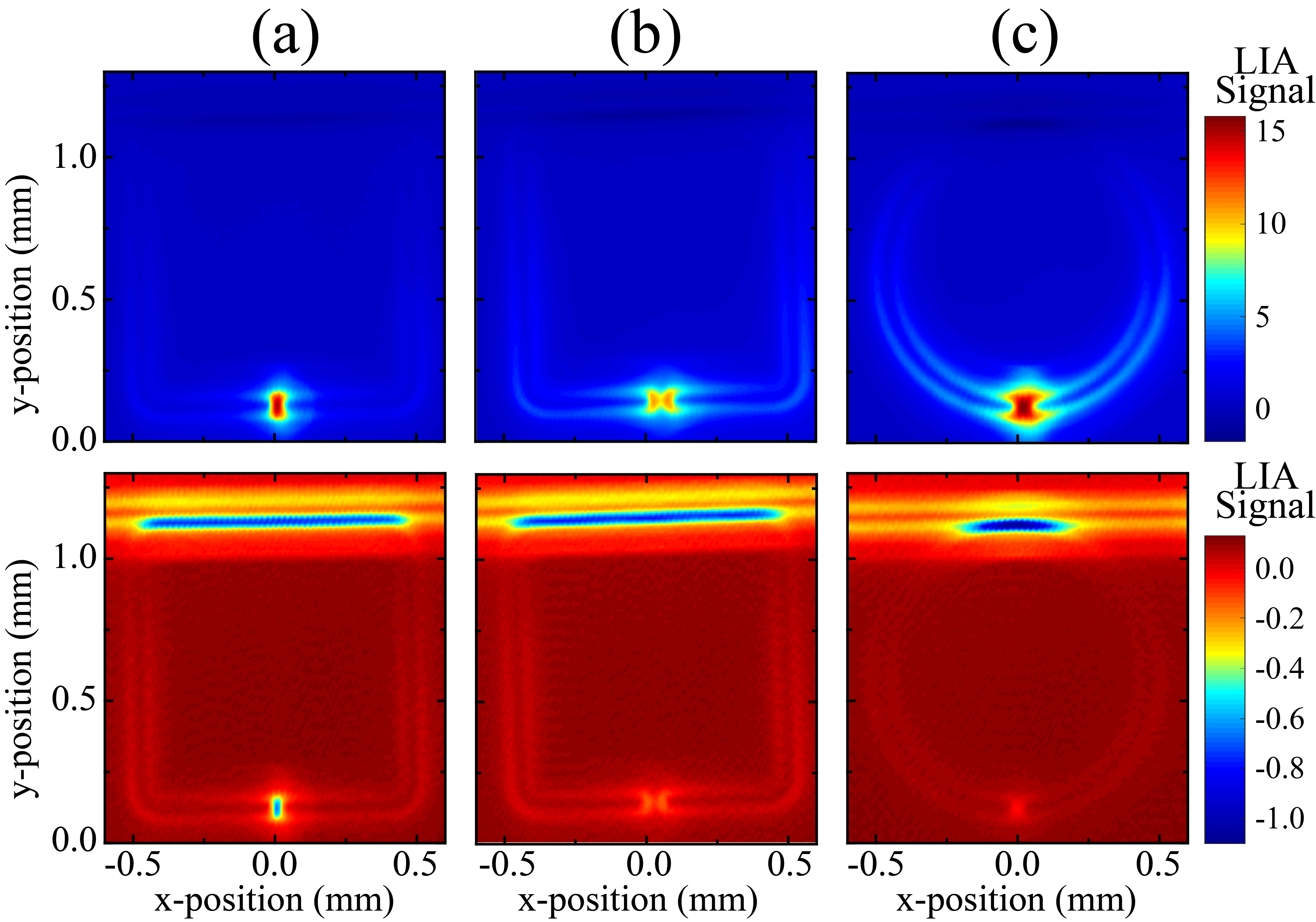
92. “Measurement of carrier lifetime in micron-scaled materials using resonant microwave circuits“, Sukrith Dev, Yinan Wang, Kyounghwan Kim, Marziyeh Zamiri, Clark Kadlec, Michael Goldflam, Samuel Hawkins, Eric Shaner, Jin Kim, Sanjay Krishna, Monica Allen, Jeffery Allen, Emanuel Tutuc, Daniel Wasserman, Nat. Commun., 10, (2019).
91. “Monochromatic Multimode Antennas on Epsilon‐Near‐Zero Materials“, Owen Dominguez, Leland Nordin, Junchi Lu, Kaijun Feng, Daniel Wasserman, and Anthony J. Hoffman, Adv. Opt. Mater. 1800826 (2019).
90. “Design and growth of multi-functional InAsP metamorphic buffers for mid-infrared quantum well lasers on InP“, D. Jung, L. Yu, S. Dev, D. Wasserman, M.L. Lee, J. Appl. Phys. 125, 082537 (2019)

2018
89. “Metal germanides for practical on-chip plasmonics in the mid infrared“, E.M. Smith, W.H. Streyer, N. Nader, S. Vangala, G. Grzybowski, R. Soref, D. Wasserman, and J.W. Cleary, Opt. Mater. Express, 8, 968 (2018)
88. “Ultra-thin enhanced-absorption long-wave infrared detectors“, Shaohua Wang, Narae Yoon, Abhilasha Kamboj, Priyanka Petluru, Wanhua Zheng, and Daniel Wasserman, Appl. Phys. Lett., 112, 091104 (2018).
87. “Optical Mapping of RF Field Profiles in Resonant Microwave Circuits”, Sukrith Dev, Runyu Liu, Jeffery W. Allen, Monica S. Allen, Brett R. Wenner and Daniel Wasserman, IEEE Photon. Technol. Lett., 30, 331 (2018).
2017
86. “Next Generation Mid Infrared Sources” D. Jung, S. Bank, M.L. Lee, D. Wasserman, J. Opt., 19 123001 (2017)
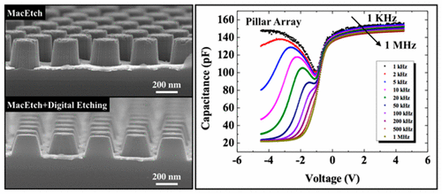
85. “Damage-Free Smooth-Sidewall InGaAs Nanopillar Array by Metal-Assisted Chemical Etching“, L. Kong, Y. Song, J.D. Kim, L. Yu, D. Wasserman, W. K. Chim, S.Y. Chiam, and X. Li, ACS Nano, 10.1021/acsnano.7b04752
84. “Mid-infrared epsilon-near-zero modes in ultra-thin phononic films“, L. Nordin, O. Dominguez, C. M. Roberts, W. Streyer, K. Feng, Z. Fang, V. A. Podolskiy, A. J. Hoffman, and D. Wasserman, Appl. Phys. Lett. 111, 091105 (2017).
83. “Modified electron beam induced current technique for in(Ga)As/InAsSb superlattice infrared detectors“, N. Yoon, C. J. Reyner, G. Ariyawansa, J. M. Duran, J. E. Scheihing, J. Mabon, and D. Wasserman, J. Appl. Phys., 122, 074503 (2017).
82. “Palladium Germanides for Mid- and Long-Wave Infrared Plasmonics“, E. Smith, W. Streyer, N. Nader, S. Vangala, R. Soref, D. Wasserman, & J. Cleary, MRS Advances, 1-6 (2017).
81. “Mid-wave infrared narrow bandwidth guided mode resonance notch filter“, Y. Zhong, Z. Goldenfeld, K. Li, W. Streyer, L. Yu, L. Nordin, N. Murphy, and D. Wasserman
Opt. Lett. 42(2), 223-226 (2017).

80. “Engineering carrier lifetimes in type-II In(Ga)Sb/InAs mid-IR emitters“, Lan Yu, Yujun Zhong, Sukrith Dev and Daniel Wasserman, Journal of Vacuum Science and Technology B, 35, 02B101 (2017).
2016
79. “Room-temperature mid-infrared quantum well lasers on multi-functional metamorphic buffers“, D. Jung, L. Yu, S. Dev, D. Wasserman and M.L. Lee, Applied Physics Letters, 109, 211101 (2016).
78. “Enhanced responsivity resonant RF photodetectors“, R. Liu, S. Dev, Y. Zhong, R. Lu, W. Streyer, J.W. Allen, M.S. Allen, B. R. Wenner, S. Gong, and D. Wasserman, Optics Express, 24, 26044-26054 (2016) DOI: 10.1364/OE.24.026044
77. “Epsilon-Near-Zero Photonic Wires“, R. Liu, C. Roberts, Y. Zhong, V.A. Podolskiy, D. Wasserman, ACS Photonics, 3 (6), pp 1045–1052 (2016) DOI: 10.1021/acsphotonics.6b00120

76. “Multiplexed infrared photodetection using resonant radio-frequency circuits” R. Liu, R. Lu, C. Roberts, S. Gong, J. W. Allen, M. S. Allen, B. R. Wenner, and D. Wasserman, Appl. Phys. Lett., 108, 061101 (2016).
75. Enhanced Optical Transmission through MacEtch-Fabricated Buried Metal Gratings”, R. Liu, X. Zhao, C. Roberts, L. Yu, P.K. Mohseni, X. Li, V. Podolskiy, and D. Wasserman, Adv. Mater., 28, 1441 (2016).
2015
74. “Engineering the Reststrahlen band with hybrid plasmon/phonon excitations“, W. Streyer, K. Feng, Y. Zhong, A.J. Hoffman, and D. Wasserman, MRS Communications, 2015
73 ” Mid-infrared electroluminescence from InAs type-I quantum wells grown on InAsP/InP metamorphic buffers “, D. Jung, L. Yu, D. Wasserman and M.L. Lee, J. Appl. Phys., 118, 183101 (2015)
72. “Photonic materials, structures and devices for Reststrahlen optics“, K. Feng, W. Streyer, Y. Zhong, A.J. Hoffman, and D. Wasserman, Opt. Express,23, A1418 (2015)
71. “Localized surface phonon polariton resonances in polar gallium nitride” , K. Feng, W. Streyer, S.M. Islam, J. Verma, D. Jena, D. Wasserman and A.J. Hoffman, Appl. Phys. Lett., 107, 081108 (2015)
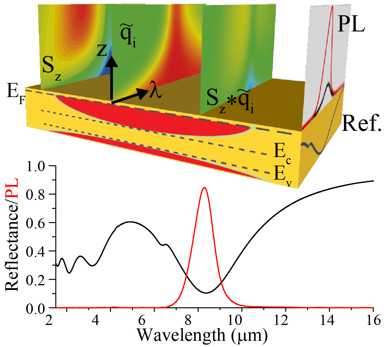
70. “Selective absorbers and thermal emitters for far-infrared wavelengths “, W. Streyer, K. Feng, Y. Zhong,A.J. Hoffman, and D. Wasserman, Appl. Phys. Lett., 107, 081105 (2015)
69. “Direct minority carrier transport characterization of InAs/InAsSb superlattice nBn photodetectors“, D. Zuo, R. Liu, D. Wasserman, J. Mabon, Z.-Y. He, Y.-H. Zhong, E.A. Kadlec, B.V. Olsen, and E.A. Shaner, Appl. Phys. Lett., 106, 071107 (2015)
68. “Review of mid-infrared plasmonic materials“, Y. Zhong, S. Devi Malagari, T. Hamilton, and D. Wasserman, J. Nanophoton. 9, 093791 (2015).
67. “Platinum germanides for mid- and long-wave infrared plasmonics”, J.W. Cleary, W.H. Streyer, N. Nader, S. Vangala, I. Avrutsky, B. Claflin, J. Hendrickson, D. Wasserman, R.E. Peale, W. Buchwald, R. Soref, Optics Express, 23, 3316-3326 (2015).
2014
66. “Design, Fabrication, and Characterization of Near-IR Gold Bowtie Nanoantenna Arrays”, H. Chen, A.M. Bhuiya, R. Liu, D. Wasserman, and K.C. Touissant, Jr., J. Phys. Chem. C, 118, 20553 (2014).
65. “Mid-infrared emission from In(Ga)Sb layers on InAs(Sb)”, R. Liu, Y. Zhong, L. Yu, H. Kim, S. Law, J.-M. Zuo, and D. Wasserman, Optics Express, 22, 24466 (2014).
64. Editorial for Special Issue on mid-infrared and THz photonics, D. Wasserman, R. Singh, and T. Akalin, J. Opt., 16, 090201 (2014).
63. “Flat mid-infrared composite plasmonic materials using lateral doping-patterned semiconductors ”, A. Rosenberg, J. Surya, R. Liu, W. Streyer, S. Law, L. Suzanne Leslie, R. Bhargava, D. Wasserman, J. Opt., 16, 094012 (2014).
62. “Controlling quantum dot energies using submonolayer bandstructure engineering”, L. Yu, D. Jung, S. Law, J. Shen, J.J. Cha, M.L. Lee, D. Wasserman, Appl. Phys. Lett., 105, 081103 (2014).
61. “Doped semiconductors with Band-Edge Plasma Frequencies”, S. Law, R. Liu, D. Wasserman, J. Vac. Sci. Technol. B, 32, 05260 1-7 (2014).
60. “Engineering absorption and blackbody radiation in the far-infrared with surface phonon polaritons on gallium phosphide“, W. Streyer, S. Law, A. Rosenberg, C. Roberts, V.A. Podolskiy, A.J. Hoffman, and D. Wasserman, Appl. Phys. Lett., 104, 131105 (2014).
59. “Epsilon-near-zero enhanced light transmission through a subwavelength slit“, S. Inampudi, D. C. Adams, T. Ribaudo, D. Slocum, S. Vangala, W.D. Goodhue, D. Wasserman, and V. A. Podolskiy, Phys. Rev. B, 89, 125119 (2014).
58. “All-Semiconductor Negative Index Plasmonic Absorbers” S Law, C. Roberts, T. Kilpatrick, L. Yu, T. Ribaudo, E.A. Shaner, V.A. Podolskiy, D Wasserman, Phys. Rev. Lett., 112, 017401 (2014).
2013
57. “Selective thermal emission from thin-film metasurfaces”, W Streyer, S Law, J Mason, DC Adams, T Jacobs, G Rooney, D Wasserman, SPIE NanoScience+ Engineering, Proc. SPIE 8808, p. 88080V-88080V-12, 20132013

56. “All-Semiconductor Plasmonic Nanoantennas for Infrared Sensing “, S. Law, L. Yu, A. Rosenberg, and D. Wasserman, Nano Lett., 13, 4560 (2013).
55. “Degenerately doped InGaBi:As as a highly conductive and transparent contact material in the infrared range”, Optics Materials Express, 3, 1197 (2013).
54. “Wafer-Scale Production of Uniform InAsyP1–y Nanowire Array on Silicon for Heterogeneous Integration“, J.C. Shin, A. Lee, P.K. Mohseni, D.Y. Kim, L. Yu, J.H. Kim, H.J. Kim, W.J. Choi, D. Wasserman, K.J. Choi, and X. Li,, ACS Nano, (2013)
53. “Near-field infrared absorption of plasmonic semiconductor microparticles studied using atomic force microscope infrared spectroscopy“, J.R. Felts, S. Law, C.M. Roberts, V. Podolskiy, D. Wasserman, and W.P. King, Appl. Phys. Lett., 102, 152110 (2013)

52. “Direct observation of minority carrier lifetime improvement in InAs/GaSb type-II superlattice photodiodes via interfacial layer control“, D. Zuo, P. Qiao, D. Wasserman, and S.L. Chuang, Appl. Phys. Lett., 102, 141107 (2013)
51. “Strong absorption and selective emission from engineered metals with dielectric coatings”, W. Streyer, S. Law, G. Rooney, T. Jacobs, and D. Wasserman, Optics Express, 21, 9113 (2013)
50. “Epitaxial growth of engineered metals for mid-infrared plasmonics”, S. Law, L. Yu, D. Wasserman, J. Vac. Sci. Technol. B, 31, 03C121 (2013).
49. “Making the mid-infrared nano with designer plasmonic materials“, S. Law, J. Felts, C. Roberts, V.A. Podolskiy, W.P. King, D. Wasserman, Proc. SPIE 8555 (2013).
48. “Towards nano-scale photonics with micro-scale photons: the opportunities and challenges of mid-infrared plasmonics”, S. Law, V. Podolskiy, and D. Wasserman, Nanophotonics,(2013)
2012
47. “2.8 um emission from type-I quantum wells grown on InAsxP12x/InP metamorphic graded buffers“, D. Jung, Y. Song, L. Yu, D. Wasserman, and M.L. Lee, Appl. Phys. Lett., 101, 251107 (2012).2012
46. “Electroluminescence from Nanosphere Lithography Fabricated Quantum Dots“, L. Yu, S. Law, D. Wasserman, Appl. Phys. Lett., 101, 103105 (2012)
45. “Mid-infrared designer metals”, S. Law, D.C. Adams, A.M. Taylor, and D. Wasserman, Optics Express, 20, 12155 (2012)
44. “Strong coupling of molecular and mid-infrared perfect absorber resonances”, J.A. Mason, G. Allen, V. podolskiy, and D. Wasserman, IEEE Photonics Technology Letters, 24, 31 (2012)
2011
43. “Enhanced Light Funneling Through Subwavelength Apertures Using Epsilon Near Zero Metamaterials”, D.C. Adams, N. Inampudi, T. Ribaudo, D. Slocum, N. Kuhta, S. Vangala, W. Goodhue, V.A. Podolskiy, and D. Wasserman, Phys. Rev. Lett., 107, 133901 (2011).2011
42. “Voltage-controlled active mid-infrared plasmonic devices” K. Anglin, T. Ribaudo, D.C. Adams, X. Qian, W.D. Goodhue, S. Dooley, E.A. Shaner and D. Wasserman, J. Appl. Phys., 109, 123103 (2011).
41. “Strong absorption and selective thermal emission from a midinfrared metamaterial” J.A. Mason, S. Smith, and D.Wasserman, Appl. Phys. Lett., 98, 241105 (2011).
40. “Multiscale beam evolution and shaping in corrugated plasmonic systems” S. Thongrattanasiri, D. C. Adams, D.Wasserman, and V. A. Podolskiy, Optics Express, 19, 9269 (2011).
39. “Observation of Rabi-Splitting from Surface Plasmon Coupled Conduction-State Transitions in Electrically-Excited InAs Quantum Dots”, B.S. Passmore, W.W. Chow, D.C. Adams, T. Ribaudo, S.A. Lyon, D. Wasserman, and E.A. Shaner, Nano-Letters, Jan (2011).

2010
38. “Selective Thermal Emission from Patterned Steel ”, J. Mason, D.C. Adams, Z. Johnson, S. Smith, A.W. Davis, and D. Wasserman, Optics Express, 18, 25912 (2010)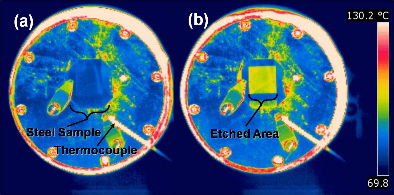
37. “Plasmonic mid-infrared beam steering”, D.C. Adams, S. Thongrattanasiri, T. Ribaudo, V. A. Podolskiy, and D. Wasserman, Appl. Phys. Lett., 96, 201112 (2010).
36. “Active Mid-Infrared Plasmonic Beam Steering Devices”, D.C. Adams, T. Ribaudo, S. Thongrattanasiri, E.A. Shaner, V. Podolskiy, and D. Wasserman, Proc. SPIE, 7756-41 (2010).
35. “High-optical-quality nanosphere lithographically formed InGaAs quantum dots using molecular beam epitaxy assisted GaAs mass transport and overgrowth”, X. Qian, S. Vangala, D. Wasserman, and W.D. Goodhue., J. Vac. Sci. Technol. B, 28(3), C3C9 (2010).

2009
34. “Spectral and spatial investigation of mid-infrared surface waves on a plasmonic grating”, T. Ribaudo, D.C. Adams, B. Passmore, E.A. Shaner and D. Wasserman, Appl. Phys. Lett., 94 201109 (2009).
33. “Mid-infrared doping tunable transmission through subwavelength metal hole arrays on InSb”, B.S. Passmore, D.G. Allen, S. R. Vangala, W.D. Goodhue, D. Wasserman, and E.A. Shaner, Opt. Express, 17 10223 (2009).
32. “Active Control and Spatial Mapping of Mid-Infrared Propagating Surface Plasmons”, T. Ribaudo, E.A. Shaner, S.S. Howard, C. Gmachl, X. Wang, F.-S. Choa, and D. Wasserman, Opt. Express, 17, 7019 (2009).
31. “Active Control of Propagating Waves on Plasmonic Surfaces”, T. Ribaudo, E.A. Shaner, S.S. Howard, C. Gmachl, X.J. Wang, F.-S. Choa, and D. Wasserman, Proc. SPIE 7221-24, 2 (2009).
30. “Room temperature midinfrared electroluminescence from InAs quantum dots“, D. Wasserman, T. Ribaudo, S.A. Lyon, S.K. Lyo, E.A. Shaner, Appl. Phys. Lett., 94, 061101 (2009).
29. “Loss mechanisms in mid-infrared extraordinary optical transmission gratings”, T. Ribaudo, K. Freitas, E.A. Shaner, J.G. Cederberg, D. Wasserman, Opt. Express 17 666 (2009).
28. “High k-space lasing in a dual-wavelength quantum cascade laser”, K.J. Franz, S. Menzel, A.J. Hoffman, D. Wasserman, J.W. Cockburn and C. Gmachl, Nature Photonics, 3, 50 (2009).
Publications (1998-2008)
27. “Active Surface Plasmons: Tuning of Surface Plasmons leads to new optoelectronic devices”, Laser Focus World, January 2008.Publications (1998-2008)
26. “Uniform InGaAs quantum dot arrays fabricated using nanosphere lithography”, X. Qian, J. Li, D. Wasserman, W.D. Goodhue, Appl. Phys. Lett., 93, 231907 (2008).
25. “Current-tunable mid-infrared extraordinary transmission gratings”, E.A. Shaner, J. Cederberg, D. Wasserman, Appl. Phys. Lett., 91, 181110 (2007)
24. Mid-Infrared doping tunable extraordinary transmission from sub-wavelength gratings”, D. Wasserman, E.A. Shaner, and J.G. Cederberg, Appl. Phys. Lett., 90, 191102 (2007)
23. “Negative Refraction in Semiconductor Metamaterials” A.J. Hoffman, L. Alekseyev, S.S. Howard, K.J. Franz, D. Wasserman, V.A. Podolskiy, E.E. Narimanov, D.L. Sivco, and C. Gmachl, Nature Materials, Published online Oct. 14th, 2007.
22. “Narrow width, low-ridge configuration for high-power quantum cascade lasers”, A. Lyahk, P. Zory, D. Wasserman, G. Shu, C. Gmachl, D. Bour Appl. Phys. Lett., 90, 141107 (2007)
21. “Evidence of cascaded emission in a dual-wavelength quantum cascade laser”, K.J. Franz, D. Wasserman, A.J. Hoffman, D.C. Jangraw, K.-T, Shiu, S.R. Forrest, and C. Gmachl, Appl. Phys. Lett., 90, 091104 (2007)
20. “Multiple wavelength polarized mid-infrared emission from InAs quantum dots”, D. Wasserman, C. Gmachl, S.A. Lyon, and E.A. Shaner, Appl. Phys. Lett. Vol. 88, p.191118 (2006).
19. ”High-Performance Quantum Cascade Lasers: Optimized Design through Waveguide and Thermal Modeling”, S. S. Howard, Z. J. Liu, D. Wasserman, A. Hoffman, T. Ko, C. F. Gmachl,IEEE J. Select. Topics Quantum Electron., 13, 1054 (2007).
18. “Room Temperature Continuous-wave Quantum Cascade Lasers Grown by MOCVD without Lateral Regrowth”, Z. Liu, D. Wasserman, S.S. Howard, A.J. Hoffman, C. Gmachl, X. Wang, T. Tanbun-Ek, L. Cheng, and Fow-Sen Choa, IEEE Photonics Technology Letters, vol. 18, p.1347 (2006).
17. “Anomalous spin polarization of GaAs two-dimensional hole systems”, R. Winkler, E. Tutuc, S.J. Papadakis, S. Melinte, M. Shayegan, D. Wasserman, and S.A. Lyon, Phys. Rev. B, vol. 72, p.195321 (2005).
16. “Electronic anti-Stokes–Raman emission in quantum-cascade lasers”, A. A Gomez-Iglesias, D. Wasserman, C. Gmachl, A. Belyanin, and D.L. Sivco, Appl. Phys. Lett., vol. 87, p. 261113 (2005).
15. “6 nm half-pitch lines and 0.04μm2 static random access memory patterns by nanoimprint lithography”, M.D. Austin, W. Zhang, H.X. Ge. D. Wasserman, S.A. Lyon, and S.Y. Chou, Nanotech., Vol 8, p.1058 (2005).
14. “Cleaved-edge overgrowth of aligned quantum dots on strained layers of InGaAs”, D. Wasserman and S. A. Lyon, Appl. Phys.Lett., Vol 85, p.5352 (2004).
13. “Scanning near-field photoluminescence mapping of (110) InAs-GaAs self-assembled quantum dots”, M. Hadjipanayi, A.C. Maciel, J.F. Ryan, D. Wasserman, and S.A. Lyon, Appl. Phys. Lett., Vol.85, p.2535 (2004).
12. “Fabrication of 5nm linewidth and 14 nm pitch features by nanoimprint lithography”, Michael D. Austin, Haixiong Ge, Wei Wu, Mingtao Li, Zhaoning Yu, D. Wasserman, S.A. Lyon, and Stephen Y. Chou, Appl. Phys. Lett., Vol 84, p.5299 (2004).
11. “Formation of self-assembled quantum dots on (110) GaAs Substrates”, D. Wasserman, S.A. Lyon, M. Hadjipanayi, A. Maciel, and .F. Ryan, Appl. Phys. Lett.. Vol. 83, p.5050 (2003).
10. “Negative differential Rashba effect in two-dimensional hole systems”, B. Habib, E. Tutuc, S. Melinte, M. Shayegan, D. Wasserman, S.A. Lyon, and R. Winkler, Appl. Phys. Lett., Vol. 85, p.3151 (2004).
9. “Characterization of GaAs grown by molecular beam epitaxy on vicinal Ge(100) substrates”, A. Wan, V. Menon, S.R. Forrest, D. Wasserman, S. A. Lyon, and A. Kahn, J. Vac. Sci. Technol. B, Vol.22, p.1893 (2004).
8. “Spin splitting in GaAs (100) two-dimensional holes”, B. Habib, E. Tutuc, S. Melinte, M. Shayegan, D. Wasserman, S. A. Lyon, and R. Winkler, Phys. Rev. B, Vol.69, p.113311 (2004).
7. “Mid-infrared luminescence from InAs quantum dots in unipolar devices”, D. Wasserman and S.A. Lyon, Appl. Phys. Lett., Vol. 81, p.2848 (2002).
6. “Doping Tunable Enhanced Extraordinary Optical Transmission Gratings”, D. Wasserman, J. Cederberg, and E.A. Shaner, Proc. SPIE 6760, 67600A (2007).
5. “MOCVD growth and regrowth of quantum cascade lasers”, F.-S. Choa, L. Cheng, X. Ji, Z. Liu, D. Wasserman, S.S. Howard, C.F. Gmachl, X. Wang, J. Fan, and J. Khurgin, Proc. SPIE 6485, 64850N (2007).
4. “Mid-infrared electroluminescence from InAs quantum dots”, D. Wasserman, S.A. Lyon, C. Gmachl, J. Cederberg, and E.A. Shaner, Proc. SPIE Vol. 6386, 63860E (2006)
3. “Mid-infrared electroluminescence from InAs quantum dots in p-n junctions and unipolar tunneling structures” D. Wasserman and S.A. Lyon, Physica Status Solidi B, Vol. 224, p.585 (2001).
2. “Electroluminescence from III-V self-assembled quantum dots”, D. Wasserman and S.A. Lyon, Book Chapter for “The Handbook of Electroluminescent Materials”, edited by Prof. D.R. Vij, Department of Physics, Kurukshetra University, India, Institute of Physics Publishing, Bristol, U.K (2004).
1. “110 InAs Quantum Dots: Growth, Single-Dot Luminescence and Cleaved Edge Alignment”, D. Wasserman, E.A. Shaner, S.A. Lyon, M. Hadjipanayi, A.C. Maciel, and J.F. Ryan, MRS Fall 2004 Meeting Proc. “Progress in Compound Semiconductor Materials IV–Electronic and Optoelectronic Applications”, Vol. 829, (2005).