
Mid-Wave and Long-Wave Infrared Detectors
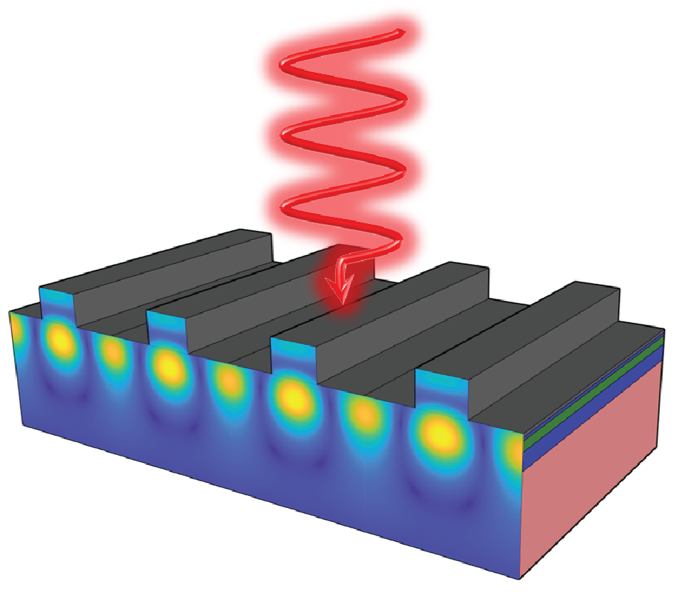
Using doped semiconductor layers as plasmon-enhanced waveguides, or plasmonic groundplanes, we have demonstrated strong enhancement of mid-wave and long-wave infrared absorption in ultra-thin detector structures. This work has resulted in room temperature operation of MWIR detectors at 4.6 micron operating wavelength, and high specific detectivity long wave infrared detectors operating at temperatures as high as 230K.
Relevant Publications
“Room-Temperature Mid-Wave Infrared Guided Mode Resonance Photodetectors for Focal Plane Arrays“, N.C. Mansfield, M. Bergthold, Y. Tischenko, S. Purkait, Y. Magendzo Behar, E. Chow, Edmond and A. Francis, V.A. Podolskiy, and D. Wasserman, IEEE Journal of Selected Topics in Quantum Electronics, 32(3), 3800509 (2026).
“Dark current mechanisms in ultra-thin mid-wave infrared detectors“, Yadviga Tischenko, Noah C. Mansfield, Morgan Bergthold, Felix A. Estevez H., Aaron J. Muhowski, Wesley T. Coon, Samuel D. Hawkins, Sreeja Purkait, Viktor A. Podolskiy, and Daniel Wasserman, J. Appl. Phys. 138, 153101 (2025)
“Room temperature mid-wave infrared guided mode resonance InAsSb photodetectors“, N. C. Mansfield, Y. Tischenko, M. Bergthold, S. Purkait; A. Raju; A. Kamboj, V. A. Podolskiy, and D. Wasserman, Applied Physics Letters (Special Collection: Mid and Long Wavelength Infrared Photonics, Materials, and Devices), 125, 171107 (2024).
“All-epitaxial guided-mode resonance mid-wave infrared detectors”, A. Kamboj, L. Nordin, P. Petluru, A. J. Muhowski, D. N. Woolf, and D. Wasserman, Appl. Phys. Lett. 118, 201102 (2021).
“Room-Temperature Mid-Wave Infrared Guided-Mode Resonance Detectors“, Abhilasha Kamboj, Leland Nordin, Aaron J. Muhowski, David Woolf, and Daniel Wasserman, IEEE Photonics Technology Letters, 34, 615 (2022).
“High operating temperature plasmonic infrared detectors“, Leland Nordin, Aaron J. Muhowski, and Daniel Wasserman, Applied Physics Letters, 120, 101103 (2022).
“Ultra-thin plasmonic detectors“, Leland Nordin, Priyanka Petluru, Abhilasha Kamboj, Aaron J. Muhowski, and Daniel Wasserman, Optica, 8, 1545 (2021).
Ultra-Fast Modulation of Self-Assembled Mid-IR Metasurfaces (With Milliron, Truskett Groups at UMich)
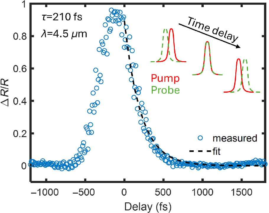
We have demonstrated that strong enhancement of absorption in monolayer tin-doped indium oxide (ITO) nano-crystals can be achieved when the monolayer NC layer is coupled to an open cavity configuration. Such an approach can give perfect absorption across a wide range of mid-IR wavelengths. However, when these structures are illuminated with light, their optical properties change drastically. We have show that under resonant illumination, absolute reflectivity can change by as much as 70%, with a recovery time in the femto-second range. This opens the door to a wide range of applications, including mode-locking of mid-IR lasers and femto-second modulation of infrared signals.
Relevant Publications:
“Self-assembled mid-infrared metasurfaces for high-contrast femtosecond switching”, Zarko Sakotic, Madeline Brown, Woo Je Chang, Lauralee E. Hurst, Noah Mansfield, Tanay Paul, Thomas M. Truskett, Monica Allen, Jeffery Allen, Delia J. Milliron, Daniel Wasserman, Advanced Photonics, 8, 026001 (2026).
“Ultrastrong Coupling by Assembling Plasmonic Metal Oxide Nanocrystals in Open Cavities”, W.J. Chang, B. Roman, T. Paul, Z. Sakotic, P. Vora, K. Kim, D. Wasserman, T. Truskett, D. Milliron, ACS Nano, 19 12332 (2025).
“Plasmonic Metal Oxide Nanocrystals as Building Blocks for Infrared Metasurfaces“,
Woo Je Chang, Allison M. Green, Zarko Sakotic, Daniel Wasserman, Thomas M. Truskett, and Delia J. Milliron, Accounts of Materials Research, 6, 104–113 (2025)
“Structural Order and Plasmonic Response of Nanoparticle Monolayers“, Allison M. Green, Woo Je Chang, Zachary M. Sherman, Zarko Sakotic, Kihoon Kim, Daniel Wasserman, Delia J. Milliron, and Thomas M. Truskett, ACS Photonics (2024)
“Wavelength Tunable Infrared Perfect Absorption in Plasmonic Nanocrystal Monolayers”, Woo Je Chang, Zarko Sakotic, Alexander Ware, Allison M. Green, Benjamin J. Roman, Kihoon Kim, Thomas M. Truskett, Daniel Wasserman, and Delia J. Milliron, ACS Nano, 18, 972 (2024).
Atomic-scale Manipulations of Interband Optical Nonlinearities, with Bank & Demkov (UT Austin), Capasso (Harvard), Alu (CUNY) and Pan (UC Irvine); AFOSR MURI
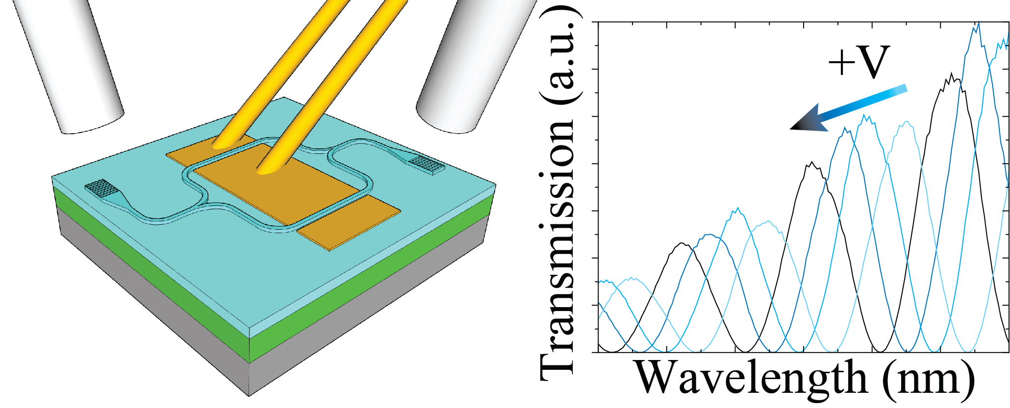
We are studying the fundamental science associated with the atomic scale design of nonlinear optical materials. Combining expertise in fundamental materials simulation/design, epitaxial materials growth, characterization, and nanophotonics we seek to expand the palate of nonlinear optical materials available to the photonics community and redefine the levels of achievable nonlinearities over technologically-important wavelength ranges. Specifically, our group has ben working with the Demkov group in the Physic Department at UT Austin to characterize barium titanate (BTO) as a nonlinear material for photonic integrated circuits. We have demonstrated monolithic BTO modulators with strong modulation and small footprints, with the potential for compact and low-power electro-optic modulators and phase shifters. We have also shown record low loss in BTO waveguides and resonators, thermo-optic modulation of BTO modulators, and dynamic control of outcoupled polarization from BTO modulated metasurfaces. In collaboration with the Bank and Alu groups, we are characterizing the nonlinear response (specifically second harmonic generation) in heterostructures grown from digital alloy materials. See more about our MURI effort here: https://sites.utexas.edu/atoms-ions/
Relevant Publications
“Dynamic Control of Polarization States with Barium Titanate Integrated Photonic Devices”, D. Krueger, L. Tian, D. Hungund, H.G. Kim, A. Raju, A. Posadas, A.A. Demkov, and D. Wasserman, Appl. Phys. Lett., 128, 161106 (2026).
“Thermo-Optic Control of Barium Titanate Modulators on Silicon-on-Insulator Substrates“, Hee Gon Kim, A. Raju, L. Tian, D. Krueger, A. Posadas, A. A. Demkov, and D. Wasserman, IEEE Photonics Technology Letters, 38, 819 (2026).
“High-Q Monolithic Ring Resonators in Low-Loss Barium Titanate on Silicon“, Amogh Raju, Divya Hungund, Dan Krueger, Zuoming Dong, Zarko Sakotic, Agham B. Posadas, Alexander A. Demkov, Daniel Wasserman, Laser and Photonics Reviews, 2402086 (2025).
“Microstructural analysis and electro-optic properties of thick epitaxial BaTiO3 films integrated on silicon (001)“, Marc Reynaud, Zuoming Dong, Hyoju Park, Wente Li, Agham B. Posadas, Jamie H. Warner, Daniel Wasserman, and Alexander A. Demkov, Phys. Rev. Materials 6, 095201 (2022).
“Monolithic Barium Titanate Modulators on Silicon-on-Insulator Substrates”, Zuoming Dong, Amogh Raju, Agham B. Posadas, Marc Reynaud, Alexander A. Demkov, and Daniel M. Wasserman, ACS Photonics (2023)
Spectrally Tunable Infrared Sensing using Lithium Niobate Optomechanical Resonators, with Povinelli, Yu, Habif (USC) and Lu (UT Austin); DARPA OpTIm program
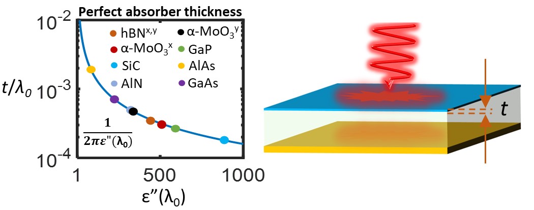
We are exploring designs for efficient mid-wave infrared absorption in ultra-thin (less than one-hundredth of a wavelength) films for high-speed and high-efficiency bolometric detection with optical read-out. In this work we are exploring absorber designs using absorbing material only nano-meters in thickness. We have developed a straightforward analytical model for the thickness required to achieve perfect absorption in thin films integrated into resonant cavity structures. We are working with Ruochen Lu’s group at UT Austin to build such absorbers on lithium niobate thin film resonators and integrate these resonators with optical read-out mechanisms.
Relevant Publications
“Suspended, Polarization-Dependent, Subwavelength-Perforated Metal Absorber for Mid-Infrared Bolometry“, Silvia Guadagnini, Zarko Sakotic, Yue Yu, Mengjie Yu, Daniel Wasserman, and Michelle L. Povinelli, Nano Letters (2025).
“Decoupling absorption and radiative cooling in mid-wave infrared bolometric elements” Alexander Ware, Morgan Bergthold, Noah Mansfield, Zarko Sakotic, Ethan A. Scott, C. Thomas Harris, and Daniel Wasserman, Optics Letters, 48, 3155-3158 (2023).
“Perfect Absorption at the Ultimate Thickness Limit in Planar Films“, Zarko Sakotic, Alexander Ware, Michelle Povinelli, and Daniel Wasserman, ACS Photonics (2023).
“Wavelength Tunable Infrared Perfect Absorption in Plasmonic Nanocrystal Monolayers”, Woo Je Chang, Zarko Sakotic, Alexander Ware, Allison M. Green, Benjamin J. Roman, Kihoon Kim, Thomas M. Truskett, Daniel Wasserman, and Delia J. Milliron, ACS Nano (2023).
Monolithic Integration of Optoelectronic and Plasmonic Materials for Mid-IR Optoelectronics
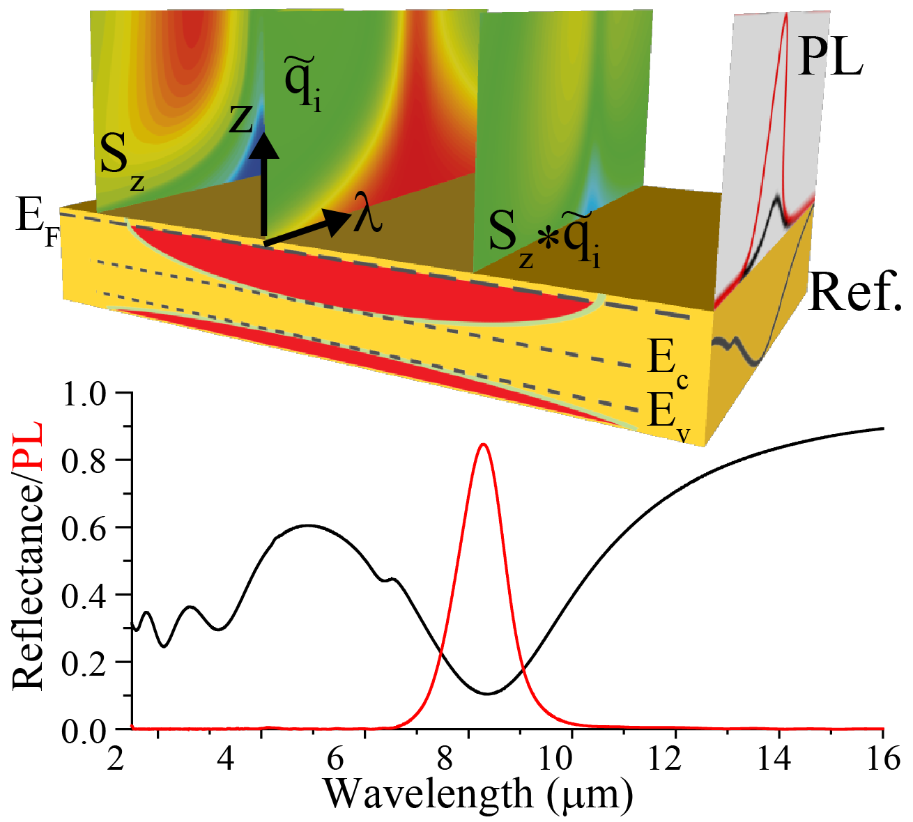
The field of plasmonics has promised a broad range of transformational advances in optics and optoelectronics, including but not limited to, on-chip sub-diffraction limited waveguiding, higher efficiency photovoltaics, sub-diffraction limit and ultra-efficient emitters, and enhanced sensitivity sensor systems. Research efforts on the above have largely focused on the near-infrared and visible wavelengths of the electromagnetic spectrum (400 nm – 3um), where efficient emitters abound, and the introduction of plasmonic materials generally results in decreased emission efficiency (even if other benefits, such as sub-wavelength confinement, are demonstrated). The mid-IR (3 – 30 um), on the other hand, is a wavelength range largely devoid of efficient emitters, where plasmonics can be leveraged to improve, not degrade, emitter efficiency. The mid-IR is also a wavelength range where high quality plasmonic materials and quantum engineered and nanostructured emitters can be grown epitaxially in the same material system. Our group utilizes the highly-doped semiconductor ‘metals’ platform, combined with quantum engineered active regions and patterned epitaxial growth, to investigate light-matter interaction at the nano length scale with micron-scale wavelengths.
Relevant Publications
“Epitaxial Mid-IR Nanophotonic Optoelectronics“, Leland Nordin and Daniel Wasserman, Applied Physics Letters, 120, 220501 (2022).
“All-epitaxial, laterally structured plasmonic materials“, Appl. Phys. Lett. 120, 161103 (2022).
“All-epitaxial long-range surface plasmon polariton structures with integrated active materials“, L. Nordin*, P. Petluru*, A.J. Muhowski, E.A. Shaner, and Daniel Wasserman, J. Appl. Phys., 129, 113102 (2021).
“Enhanced room temperature infrared LEDs using monolithically integrated plasmonic materials“, A.F. Briggs, L. Nordin, A.J. Muhowski, E. Simmons, P. Dhingra, M.L. Lee, V.A. Podolskiy, D. Wasserman, and S.R. Bank, Optica 7, 1355-1358 (2020)
Previous Programs
Mid-IR Quantum Dot LEDs (with Nanohmics, funded by AFRL)
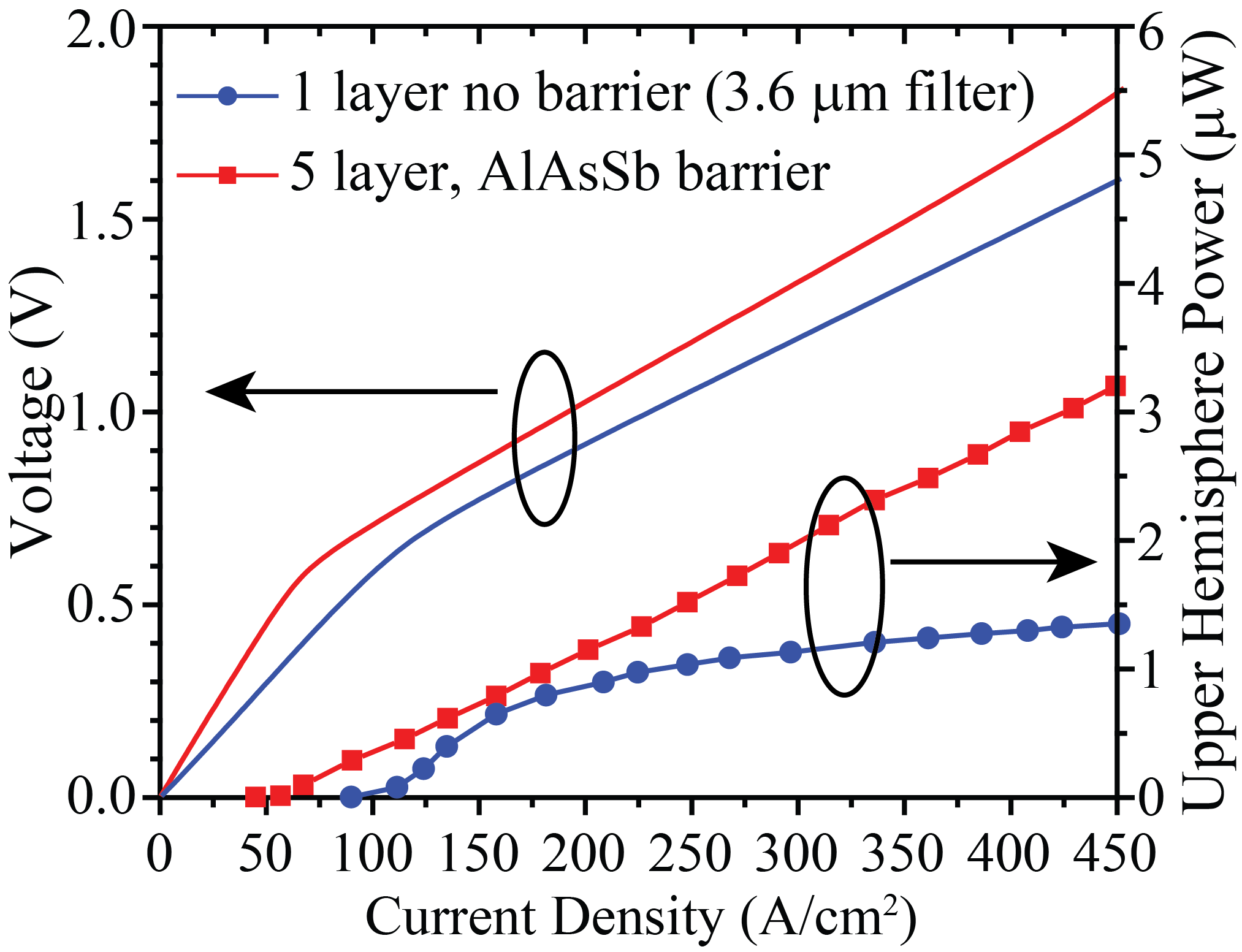
The low cost and high efficiency of visible and near-IR light emitting diodes have played a vital role in a number of applications, including solid state lighting and consumer electronics, allowing for efficient incoherent light emission from semiconductor materials. However, similar efficiencies are difficult to achieve in the longer wavelength mid-IR, where LEDs might have potential applications in low-cost sensing platforms and “thermal television” screens for security and defense applications. In this program we are investigating the utility of semiconductor quantum dots, nanometer scale structures embedded in a host material, capable of emitting light at mid-IR wavelengths. We are looking to develop new device architectures and growth parameters in order to increase emission efficiency and temperature performance for LEDs operating in the 4-6 um range.
Relevant Publications
“Cascaded InGaSb quantum dot LEDs“, A. J. Muhowski, A. Kamboj, A.F. Briggs, L. Nordin, S. R. Bank, and D. Wasserman, J. Appl. Phys. 131, 043105 (2022).
“Engineering carrier lifetimes in type-II In(Ga)Sb/InAs mid-IR emitters“, Lan Yu, Yujun Zhong, Sukrith Dev and Daniel Wasserman, Journal of Vacuum Science and Technology B, 35, 02B101 (2017).
“Mid-infrared emission from In(Ga)Sb layers on InAs(Sb)”, R. Liu, Y. Zhong, L. Yu, H. Kim, S. Law, J.-M. Zuo, and D. Wasserman, Optics Express, 22, 24466 (2014).
Semiconductor Heterostructure Platform for Active Hyperbolic Materials (with Profs. Podolskiy at UMass Lowell, Gmachl at Princeton University and Narimanov at Purdue University)
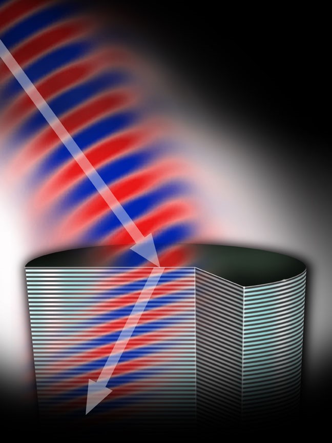
In this program we are looking to develop a new material platform for manipulation of mid-IR light and use this platform to perform a comprehensive study not only of the interplay between material properties and metamaterial geometry, but also of light propagation, emission, and absorption in complex [quantum-] plasmonic metamaterials. The materials developed in the proposed research will be directly applicable to the development of new classes of optical components, while the developed analytical and numerical tools will be applicable to understanding the complex behavior of a wide class of plasmonic materials from noble metals at visible frequencies to transparent oxides in the near-IR to doped semiconductors in the mid-IR and THz, and will potentially be utilized in the design of future detectors, emitters, and other components.
Relevant Publications
“Extending plasmonic response to the mid-wave infrared with all-epitaxial composites“, Aaron J. Muhowski, Evan Simmons, Kun Li, Evgenii E. Narimanov, Viktor A. Podolskiy, and Daniel Wasserman, Opt. Lett. 47(4), 973-976 (2022).
“Subdiffraction Limited Photonic Funneling of Light“, K. Li, E. Simmons, A.F. Briggs, L. Nordin, J. Xu, V. Podolskiy and D. Wasserman, Advanced Optical Materials, 2001321 (2020)
“Ballistic Metamaterials“, Kun Li, Evan Simmons, Andrew F. Briggs, Seth R. Bank, Daniel Wasserman, Viktor A. Podolskiy, and Evgenii E. Narimanov, Optica, 7, 1773-1780 (2020).
“Negative Refraction in Semiconductor Metamaterials” A.J. Hoffman, L. Alekseyev, S.S. Howard, K.J. Franz, D. Wasserman, V.A. Podolskiy, E.E. Narimanov, D.L. Sivco, and C. Gmachl, Nature Materials, 2007.
Resonant RF Circuits for Infrared Detection and Material Metrology (with Drs. M Allen, J. Allen, and B. Wenner at AFRL)
The rapid growth of wireless communication technologies has resulted in an abundance of new chip-scale radio-frequency (RF) structures and devices, with a corresponding decrease in RF device cost. New technologies and the scaling of RF components hold the potential to continue the shrinking of the “THz gap” between optical and optoelectronic devices (typically operating at >100THz frequencies) and electronic devices, now operating up to 100’s of GHz and even THz frequencies. There is thus increasing interest in devices and architectures that are able to merge RF and optical capabilities, linking these two technologies that make the foundation of our modern communication infrastructure. At the same time, the greater accessibility of RF components offers new opportunities for materials and device metrology at lower costs. These components could enable efficient and cost-effective high-frequency measurement of device performance and material response across a range of optical materials and optoelectronic device architectures. In this project we are demonstrating high operating temperature detectors where incident light, absorbed by a semiconductor material in an RF resonant circuit, alters the local conductivity (or complex permittivity) of the resonant microwave circuit and is read out with an RF signal. Our approach offers a path towards multiplexed, multiple-wavelength and high-speed or high-sensitivity detection of incident radiation.

Relevant Publications:
“Measurement of carrier lifetime in micron-scaled materials using resonant microwave circuits“, Sukrith Dev, Yinan Wang, Kyounghwan Kim, Marziyeh Zamiri, Clark Kadlec, Michael Goldflam, Samuel Hawkins, Eric Shaner, Jin Kim, Sanjay Krishna, Monica Allen, Jeffery Allen, Emanuel Tutuc, Daniel Wasserman, Nat. Commun., 10, (2019).
“Optical Mapping of RF Field Profiles in Resonant Microwave Circuits”, Sukrith Dev, Runyu Liu, Jeffery W. Allen, Monica S. Allen, Brett R. Wenner and Daniel Wasserman, IEEE Photon. Technol. Lett., 30, 331 (2018).
“Enhanced responsivity resonant RF photodetectors“, R. Liu, S. Dev, Y. Zhong, R. Lu, W. Streyer, J.W. Allen, M.S. Allen, B. R. Wenner, S. Gong, and D. Wasserman, Optics Express, 24, 26044-26054 (2016) DOI: 10.1364/OE.24.026044
“Multiplexed infrared photodetection using resonant radio-frequency circuits” R. Liu, R. Lu, C. Roberts, S. Gong, J. W. Allen, M. S. Allen, B. R. Wenner, and D. Wasserman, Appl. Phys. Lett., 108, 061101 (2016).
THz Switching with Degenerately Doped Semiconductor Devices (with Prof. Genov at La. Tech.)
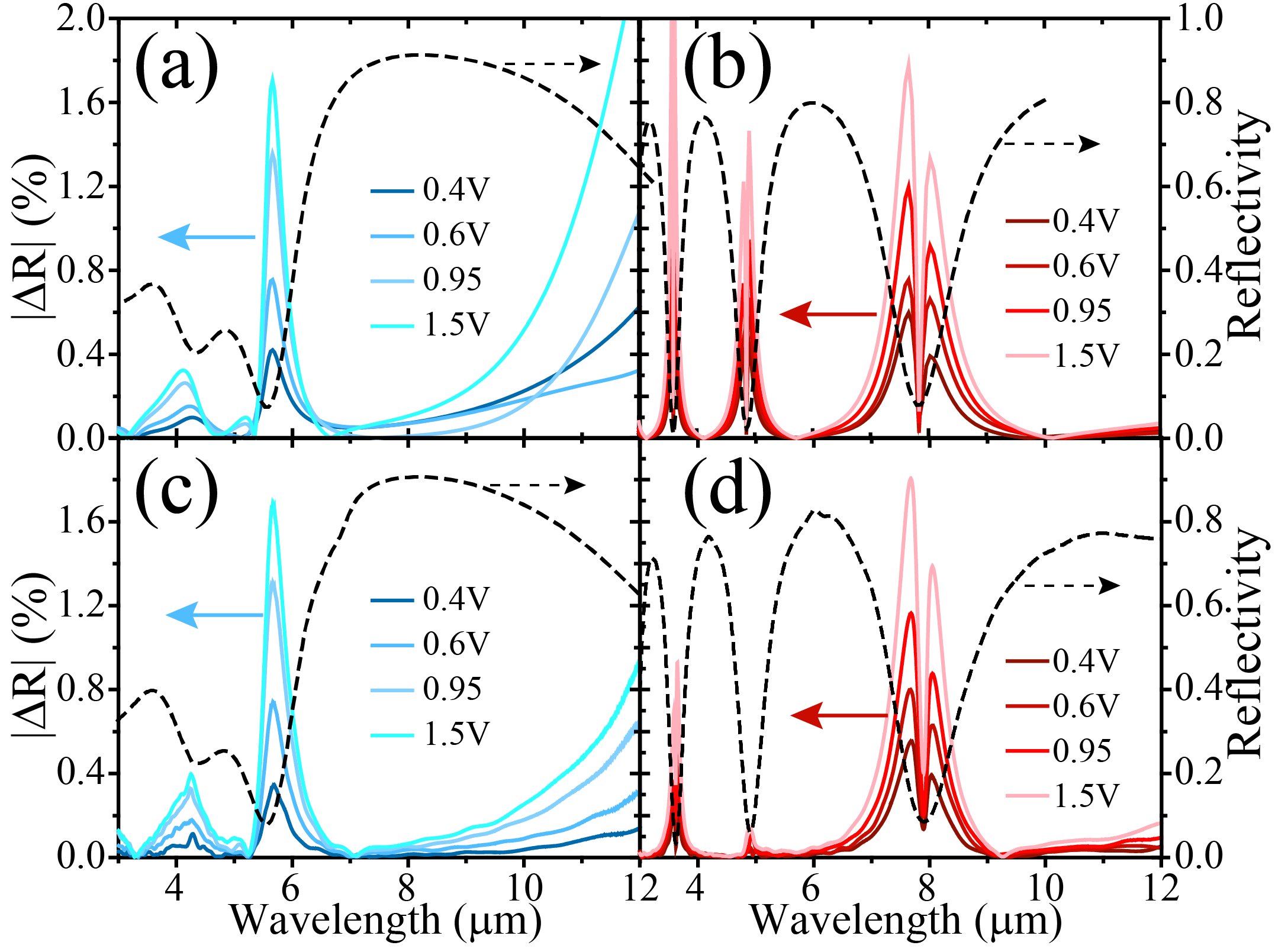
Our group has a long-standing interest in the use of highly-doped semiconductors as long-wavelength plasmonic materials for IR applications. Such materials offer plasma frequencies across the mid-IR by control of dopant, and thus free carrier, concentrations. The high carrier concentrations required for plasmonic behavior in the mid-IR can be achieved in Si by top-down ion implantation or spin-doping, or in III-V materials during (bottom up) epitaxial growth. Both the top-down and bottom-up approaches allow for the development of semiconductor device architectures with integrated plasmonic materials. The former allows for direct integration of mid-IR plasmonic systems with Si electronics, while the latter offers the potential for layered growth of ‘metallic’ and dielectric materials, and thus monolithic integration with mid-IR optoelectronic active regions. Either approach offers the opportunity for the development of a new generation of dynamic plasmonic devices. One such example is the proposed surface plasmon polariton diode (SPPD), an optoelectronic switch where the propagation of a surface plasmon polariton (SPP) propagating at an n++p junction is modulated by charge injection during forward biasing of the junction. Simulated performance of the SPPD suggest potential modulation of up to 98% and switching rates of 1 THz, which when combined with the SPPD’s compatibility with current semiconductor growth/fabrication techniques, offers an avenue towards high speed electrical switching of optical signals with subwavelength mode volumes. In this project we collaborate with the inventor of the SPPD to demonstrate an experimental realization of high speed switching of SPPs at degenerately doped semiconductor interfaces.
Relevant Publications
“Electrical modulation of degenerate semiconductor plasmonic interfaces“, Z. Dong, R.K. Vinnakota, A.F. Briggs, L. Nordin, S.R. Bank, D.A. Genov, and D. Wasserman, J. Appl. Phys., 126, 043101 (2019).
W. Streyer, S. Law, G. Rooney, T. Jacobs and D. Wasserman, “Strong absorption and selective emission from engineered metals with dielectric coatings,” Opt. Express, vol. 21, no. 7, p. 9113, Apr. 2013.
A. Rosenberg, J. Surya, R. Liu, W. Streyer, S. Law, L. Suzanne Leslie, R. Bhargava, D. Wasserman, “Flat mid-infrared composite plasmonic materials using lateral doping-patterned semiconductors ”, J. Opt., 16, 094012 (2014)..
S. Law, D. C. Adams, A. M. Taylor, and D. Wasserman, “Mid-infrared designer metals,” Optics Express, vol. 20, no. 11, p. 12155, May. 2012.
S. Law, L. Yu, and D. Wasserman, “Epitaxial growth of engineered metals for mid-infrared plasmonics,” J. Vac. Sci. Technol. B, vol. 31, no. 3, p. 03C121, Mar. 2013.
S. Law, T. Kilpatrick, L. Yu, T. Ribaudo, C. Roberts, V.A. Podolskiy, E.A. Shaner, and D. Wasserman, “All-Semiconductor Plasmonic Perfect Absorbers”, Phys. Rev. Lett., 112, 017401 (2014).
R.K. Vinnakota, D.A. Genov, Terahertz Optoelectronics with Surface Plasmon Polariton Diode, Sci. Rep. 4, 20–27 (2014).
R.K. Vinnakota and D.A. Genov, “Active Control of Charge Density Waves at Degenerate Semiconductor Interfaces”, Sci. Rep., 7, 10778 (2017).
Reststrahlen Band Optics (with Prof. A. Hoffman, Notre Dame)
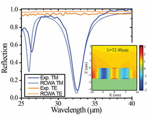
The far-infrared (far-IR) region of the electromagnetic spectrum can be considered to fill the space from the edge of the long-wave infrared (~13µm) all the way through to the mm-wave portion of the spectrum. The long-wavelength side of the far-IR is most frequently referred to as the THz wavelength range, which is of great interest for a wide variety of optoelectronic, sensing, and imaging applications. The shorter wavelength side of the far-IR (~20-100µm, which we refer to as the Reststrahlen band) unlike the THz, has received little attention thus far, despite being a wavelength range of potential interest for explosives detection, chemical and biological spectroscopy, and astrophysics applications. The exploration of any wavelength range requires an optical toolkit, consisting of sources, detectors, and optical components such as lenses, beamsplitters, polarizers, and filters. In the ~20-100µm wavelength range, such components are few and far between. In large part, this is due to the strong phonon absorption of semiconductor materials, which form the basis of most all optoelectronic devices and in the infrared, most optical materials. This thrust of my group’s research focuses on the development of materials and devices for far-IR optics. In particular, we are interested in harnessing optical phonons for a new class of opto-phononic-electronic devices and structures.
Relevant Publications:
“Monochromatic Multimode Antennas on Epsilon‐Near‐Zero Materials“, Owen Dominguez, Leland Nordin, Junchi Lu, Kaijun Feng, Daniel Wasserman, and Anthony J. Hoffman, Adv. Opt. Mater. 1800826 (2019).
“Phonon-polaritonics: enabling powerful capabilities for infrared photonics“, Stavroula Foteinopoulou, Ganga Chinna Rao Devarapu, Ganapathi S. Subramania, Sanjay Krishna, and Daniel Wasserman, Nanophotonics, (2019)
“Probing polaritons in the mid- to far-infrared“, T.G. Folland, L. Nordin, D. Wasserman, and J.D. Caldwell, Journal of Applied Physics 125, 191102 (2019)
“Mid-infrared epsilon-near-zero modes in ultra-thin phononic films“, L. Nordin, O. Dominguez, C. M. Roberts, W. Streyer, K. Feng, Z. Fang, V. A. Podolskiy, A. J. Hoffman, and D. Wasserman, Appl. Phys. Lett. 111, 091105 (2017).
“Engineering the Reststrahlen band with hybrid plasmon/phonon excitations“, W. Streyer, K. Feng, Y. Zhong, A.J. Hoffman, and D. Wasserman, MRS Communications, 2015
“Photonic materials, structures and devices for Reststrahlen optics“, K. Feng, W. Streyer, Y. Zhong, A.J. Hoffman, and D. Wasserman, Opt. Express,23, A1418 (2015)
“Localized surface phonon polariton resonances in polar gallium nitride” , K. Feng, W. Streyer, S.M. Islam, J. Verma, D. Jena, D. Wasserman and A.J. Hoffman, Appl. Phys. Lett., 107, 081108 (2015)
“Selective absorbers and thermal emitters for far-infrared wavelengths “, W. Streyer, K. Feng, Y. Zhong,A.J. Hoffman, and D. Wasserman, Appl. Phys. Lett., 107, 081105 (2015)
“Review of mid-infrared plasmonic materials“, Y. Zhong, S. Devi Malagari, T. Hamilton, and D. Wasserman, J. Nanophoton. 9, 093791 (2015).
“Engineering absorption and blackbody radiation in the far-infrared with surface phonon polaritons on gallium phosphide“, W. Streyer, S. Law, A. Rosenberg, C. Roberts, V.A. Podolskiy, A.J. Hoffman, and D. Wasserman, Appl. Phys. Lett., 104, 131105 (2014).
Mid-IR Type-II Superlattice Detectors (ARO MURI, with ASU, UNCC, GaTech, and Texas A&M)
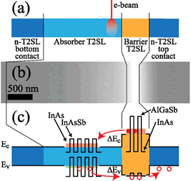
Type II superlattices (T2SLs) have undergone a significant amount of development and progress since their initial proposed use for the detection of mid- to long-wavelength infrared (MWIR, LWIR) radiation. The type-II broken band gap alignment of these heterostructures allows electrons and holes to be confined in separate but adjacent, nanometer scale thickness, material layers. When arranged in a highly periodic structure comprised of thin layers of alternating materials, known as a superlattice (SL), the carriers form minibands that have an effective band gap lower than that of the constituent materials and suited for MWIR and LWIR applications. Traditionally, InAs/GaSb has been the preferred material system for T2SL IR detectors, but recent work has also explored the use of InAs/InAsSb as well. This effort explores the characterization of carrier transport properties in T2SL devices through a variety of techniques, though primarily with the application of electron beam induced current (EBIC) measurements. For these EBIC measurements, using first principle analysis of the low-injection diffusion of carriers generated by inelastic scattering of high-energy electrons, we develop theoretical models to characterize minority carrier diffusion length and surface recombination velocity in photodetectors along the growth direction. Novel EBIC analysis of an nBn photodetector with InAs/InAsSb regions, combined with lifetime measurements through time-resolved photoluminescence (TRPL), form a comprehensive characterization of the device vertical transport properties, including mobility and diffusivity.
Relevant Publications:
“Modified electron beam induced current technique for in(Ga)As/InAsSb superlattice infrared detectors“, N. Yoon, C. J. Reyner, G. Ariyawansa, J. M. Duran, J. E. Scheihing, J. Mabon, and D. Wasserman, J. Appl. Phys., 122, 074503 (2017).
“Direct minority carrier transport characterization of InAs/InAsSb superlattice nBn photodetectors“, D. Zuo, R. Liu, D. Wasserman, J. Mabon, Z.-Y. He, Y.-H. Zhong, E.A. Kadlec, B.V. Olsen, and E.A. Shaner, Appl. Phys. Lett., 106, 071107 (2015)
“Direct observation of minority carrier lifetime improvement in InAs/GaSb type-II superlattice photodiodes via interfacial layer control“, D. Zuo, P. Qiao, D. Wasserman, and S.L. Chuang, Appl. Phys. Lett., 102, 141107 (2013)