
Defects Engineering:
In the past few years, layered materials transition metal dichalcogenides (TMDs) have attracted numerous research interests because of their extraordinary properties, such as direct band gap in monolayer samples, stable excitons and trions at room temperature, superior immunity to short channel effects, and strong spin−valley coupling, which make TMDs promising for applications in nano- and flexible electronics, photonics, and valleytronics.
For many of these TMD-based devices, it is essential to understand the physics of carrier-related interactions and to acquire carrier transport properties that determine the key performance metrics (e.g., bandwidth and responsivity), such as carrier lifetime, diffusion coefficient, and mobility. However, defects inside TMDs or from their environments (substrates and surface adsorbates) can interact with excitons/carriers and significantly affect the functionalities of the electronic devices. For example, the chalcogen vacancy defect and its related complex are able to activate additional defect-associated photoluminescence (PL) channels, which can decrease the intrinsic exciton PL efficiency. Charged impurity scattering due to either the ionized impurities inside TMDs or charge traps at the surface of the substrate has been proposed to be the dominant factor for the observed low room-temperature mobility in TMD devices. Charge traps at the TMD-gate insulator interface have also been suggested as the cause of hysteresis in TMD-based field-effect transistors. Some defects can also serve as recombination centers, assisting the recombination of the photoexcited excitons/carriers in exfoliated few-layer and multilayer TMDs via Auger scattering.
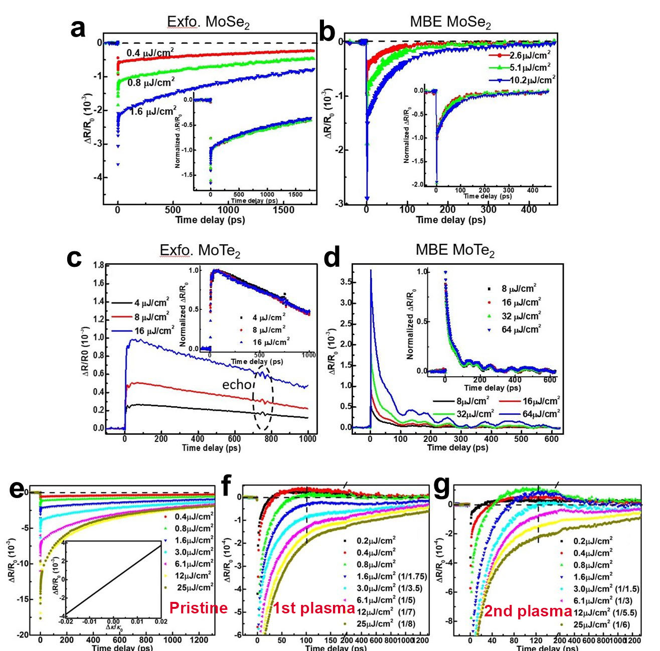
Fig a&b c&d Differential reflection signals of exfoliated TMDs (less defects) and MBE-grow TMDs (more defects) showing faster carrier recombination rate due to grain boundary/edge defects e&f&g Differential reflection signals showing the plasma-created O2 impurity’s impact on carrier dynamics by generating mid-gap defects
Nonlinear Optical Properties:
Nonlinear optics is the behavior of light in nonlinear media, where the polarization P responds nonlinearly to the electric field of the light. The nonlinearity is typically observed at high light intensities, so it remained unexplored until the discovery of lasers.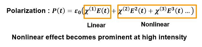
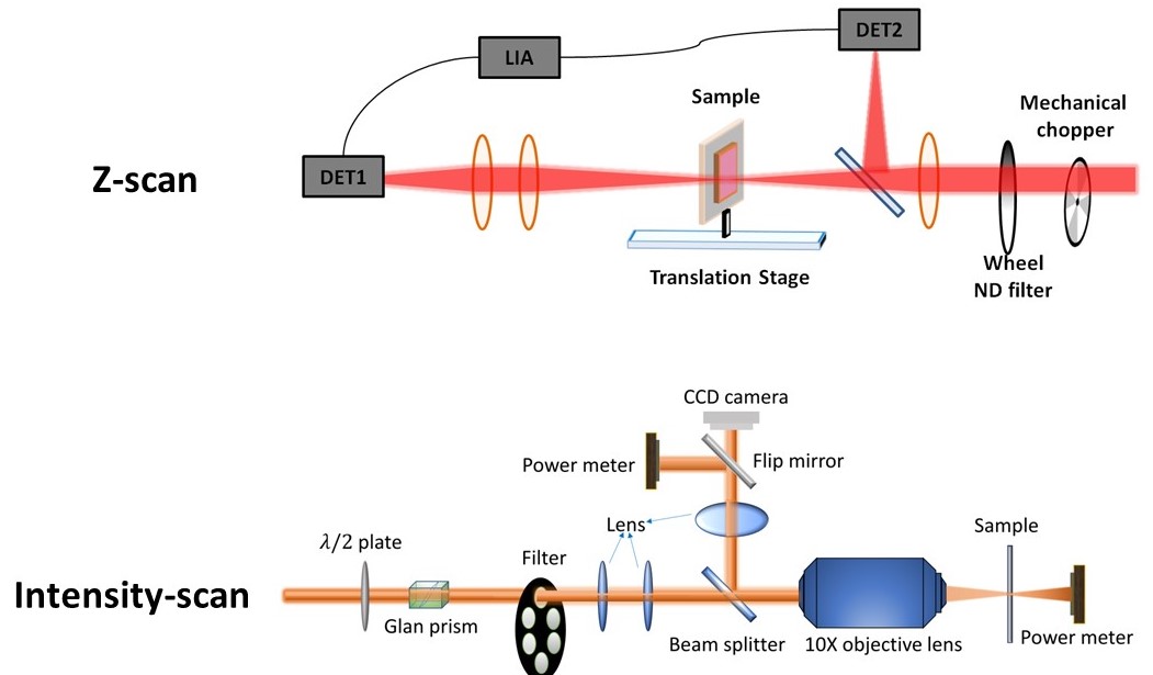
The Z-scan technique is used as a standard method to study the nonlinear optical response, where the incident laser power is fixed and the irradiance on the sample is changed by scanning the sample position around the laser focal point. In the standard Z-scan technique, a large sample size and good sample homogeneity are required. As a result, most Z-scan experiments in TMDs are conducted in solutions with suspended TMD nanoflakes, from which it is difficult to resolve the polarization‑dependent response. With the intensity-scan (I-scan) technique, where the laser irradiance is controlled by neutral density filters instead of moving the sample position, one can determine the nonlinear optical properties in inhomogeneous samples with low damage threshold. Thus, the I-scan technique is much better suited to study exfoliated or CVD-grown, single-domain 2D flakes, which usually have a very limited radiation area.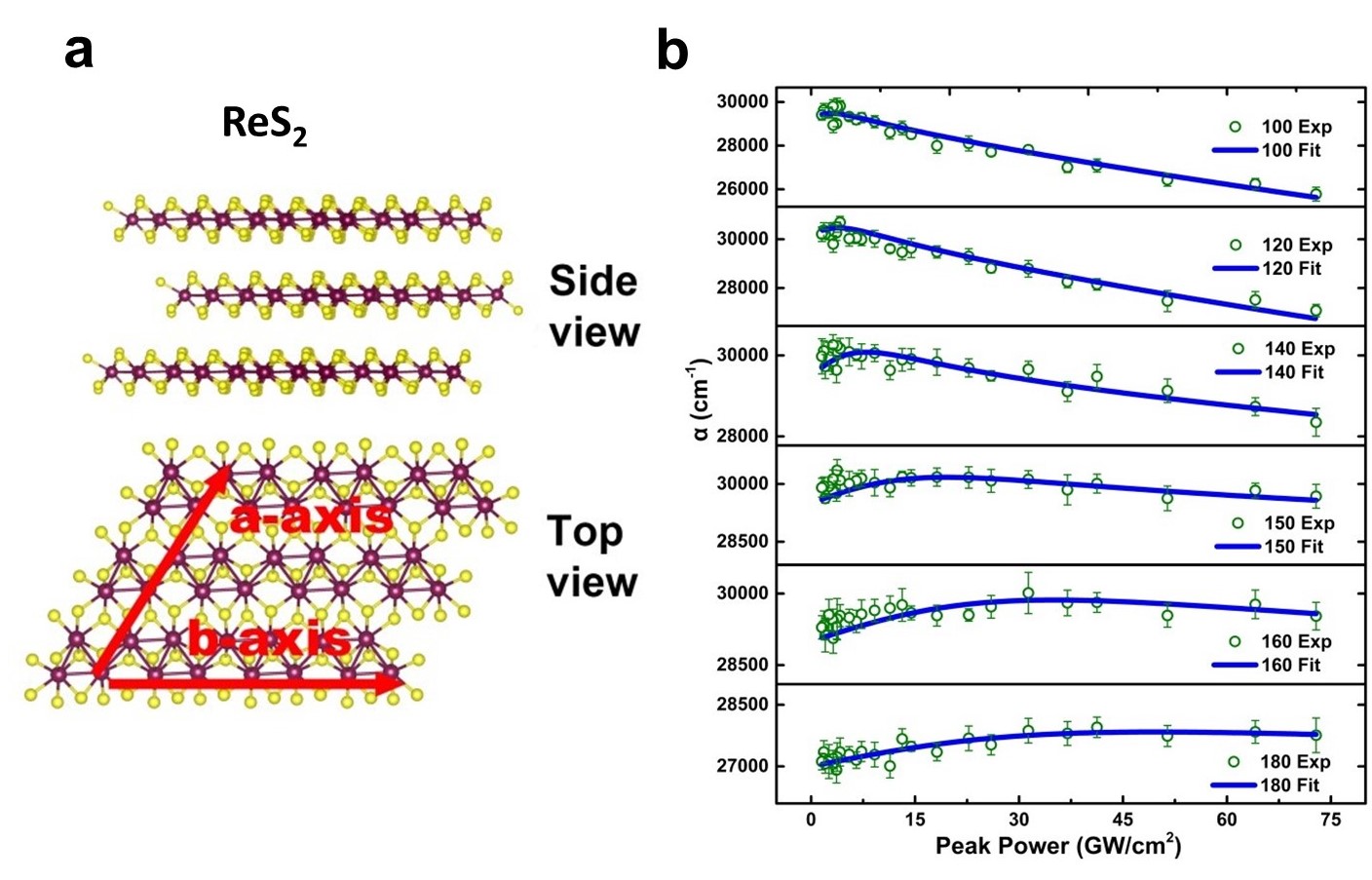
Fig a. Schematics of ReS2 crystal structure b. Absorption coefficients at increasing peak power at different polarization conditions (different angle between laser polarization and b-axis of ReS2)