
High pressure physics: High pressure could induce various novel phenomena, due to the drastic shrinkage of atomic volume, such as enhanced electronic density, overlapped electronic orbitals. High pressure physics have been undergoing a fast advance in recent years with the combination of high pressure devices with probing techniques or new materials. Diamond anvil cell (DAC), which was initially invented to simulate the high pressure environment down in the earth mantle, is utilized by researchers in condensed matter physics to explore various new phenomena, such as: high Tc superconductors, pressure induced metalization, quantum criticality, phononic properties. A diamond anvil cell (DAC) device (shown in Fig.1(a)&(b)) is composed of two opposing faced diamonds anvils. The diamond anvils along with a gasket, usually a strong and stiff metal piece (Stainless steel, Re) enclose pressure medium in a sealed chamber. DAC device with upper and lower plates are connected by four screws. The applied force is created by tightening the screws, and the uni-axial force is transformed into hydrostatic force through the pressure medium. The culet size is usually very small (several hundred microns), so with moderate force, extremely high pressure can be reached, based on the simple equation, pressure = force/area. Since the diamond windows are transparent to wide wavelength range of electromagnetic waves, many optical measurements could be achieved, such as Raman, X-ray diffraction, photoluminescence, etc. Combining DAC with optical measurements allows us to probe non-invasively the in-situ thermal and electron properties of the samples under high pressure.
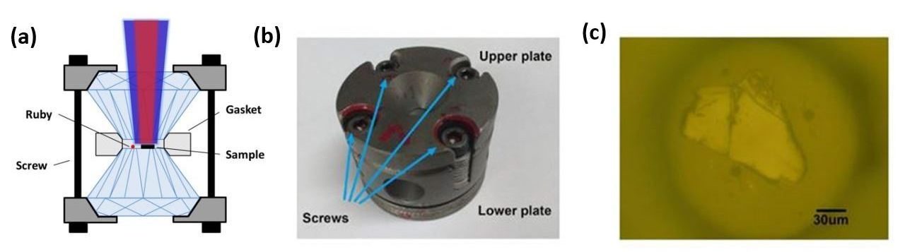
Fig. 1(a) Schematics of Diamond Anvil Cell (DAC) (b) Optical image of real DAC device (c) Optical image of MoS2 sample loaded in DAC
Project 1: Thermal Conductivity Enhancement in MoS2 under Extreme Strain [1]
Under high pressure, MoS2 transits from the semiconductor to the semi-metal state. Recently, with our optical characterization technique, we observed that pressure could significantly enhance the cross-plane thermal conductivity(Fig. 2(a)-(b)) of 2D materials due to the enhanced group velocity(Fig. 2(c)-(d)) resulting from strengthened interlayer interaction under high pressure. Our results suggest possible parallel tuning of structural, thermal, and electrical properties of VdW solids with strain in multiphysics devices. [For details of thermal conductivity measurement, please see the page “thermal transport“].
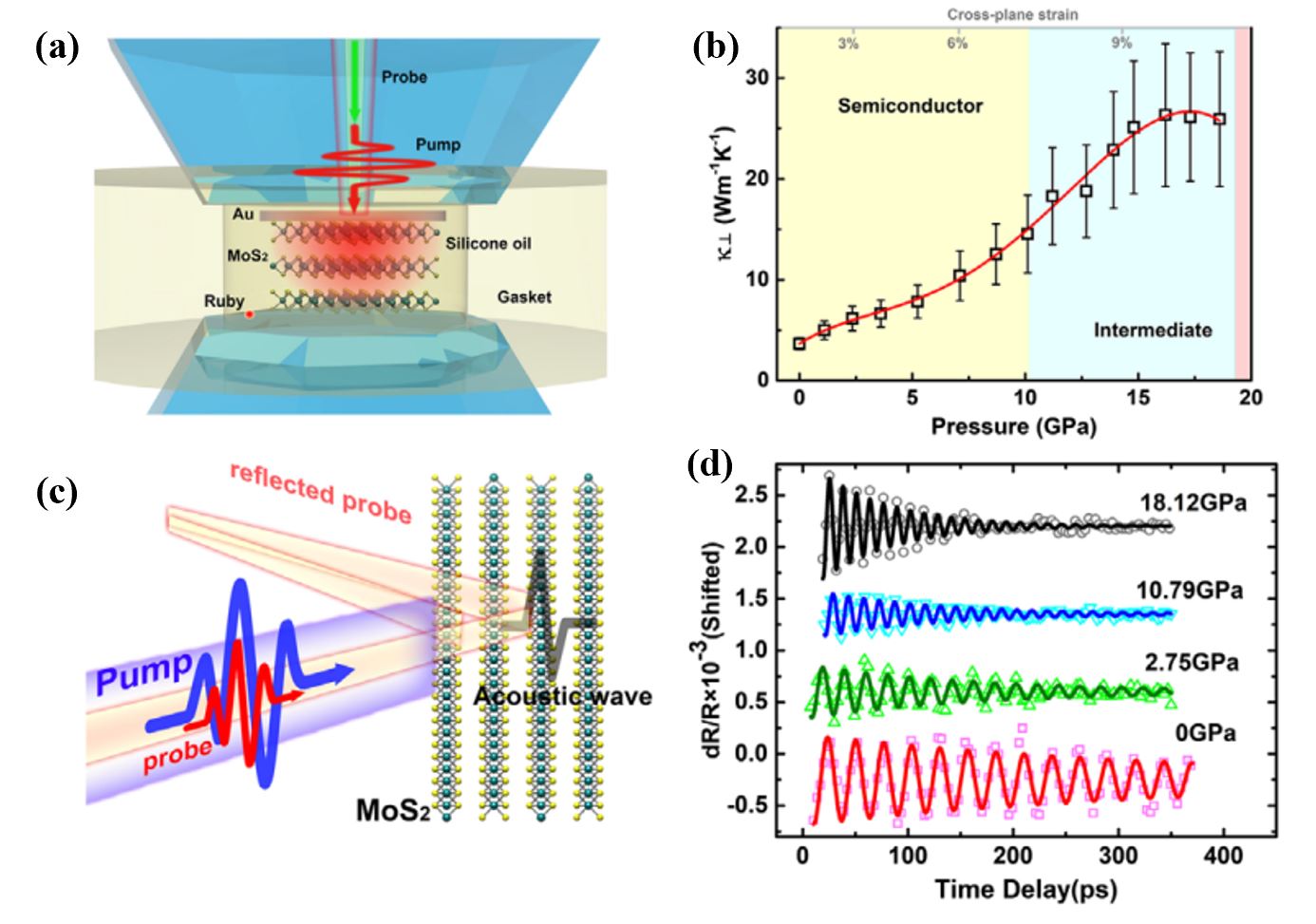
Fig. 2. (a) Schematic of thermal conductivity measurement with a diamond anvil cell integrated with a ps-TTR system. (b) Extracted cross-plane thermal conductivity (both lattice and electronic) as a function of pressure. The red curve is included only as a guide to the eye. (c) Schematic of coherent phonon scattering(CPS) measurements of coherent acoustic phonons in an uncoated MoS2 sample. (d) Pressure-dependent coherent oscillations of longitudinal acoustic phonons measured with CPS.
Project 2: Pressure-Dependent Behavior of Defect-Modulated Band Structure in Boron Arsenide(BAs) [2]
The recent observation of unusually high thermal conductivity exceeding
1000 W/mK in single-crystal boron arsenide (BAs) has led to interest in
the potential application of this semiconductor for thermal management. We reported the photoluminescence (PL) measurement of single-crystal BAs at different temperatures and pressures(Fig. 3(a)). The spectra reveal an indirect bandgap and two donor–acceptor pair (DAP) recombination transitions originated from Si and C impurities. High-pressure PL spectra show that the donor level with respect to the conduction band minimum shrinks with increasing pressure, which affects the release of free carriers from defect states.(Fig. 3(b)) These findings suggest the possibility of strain engineering of the electronic properties of BAs for application in electronic devices.
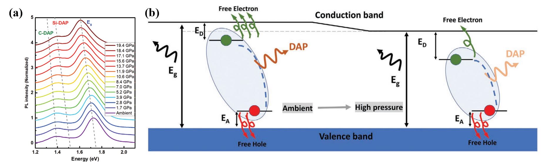
Fig. 3. (a) Experimental data of PL spectra from ambient pressure to 20 GPa. (b) Schematic picture of the pressure effect on the PL photon energy and the free carriers release. The energy levels changes are exaggerated for illustration purposes.
Project 3: Defect-modulated thermal transport behavior of BAs under high pressure [3]
Boron arsenide (BAs) is a covalent semiconductor with a theoretical intrinsic thermal conductivity approaching 1300 W/mK. The existence of defects not only limits the thermal conductivity of BAs significantly but also changes its pressure-dependent thermal transport behavior. We used both picosecond transient thermoreflectance (ps-TTR) and femtosecond time-domain thermoreflectance techniques (TDTR), and observed a non-monotonic dependence of thermal conductivity on pressure(Fig.4(a)-(c)). This trend is a result of several competing effects, including defect–phonon scattering and modification of structural defects under high pressure. Our findings reveal the complexity of the defect-modulated thermal behavior under pressure due to sample inhomogeneity and defects.
 Fig. 4. (a)-(c)Pressure-dependent thermal conductivity measured with TTR at selected sample spots on sample No. 1. Both compression (blue open circles) and decompression (red open circles) data were collected from the samples. (d) Pressure-dependent thermal conductivity measured with TDTR at different spots of sample No. 2.
[1] Meng, X., Pandey, T., Jeong, J., Fu, S., Yang, J., Chen, K., … & Wang, Y. (2019). Thermal conductivity enhancement in MoS 2 under extreme strain. Physical Review Letters, 122(15), 155901.
[2] Meng, X., Singh, A., Juneja, R., Zhang, Y., Tian, F., Ren, Z., … & Wang, Y. (2020). Pressure‐Dependent Behavior of Defect‐Modulated Band Structure in Boron Arsenide. Advanced Materials, 32(45), 2001942.
[3] Zhou, Y., Hsieh, W. P., Chen, C. C., Meng, X., Tian, F., Ren, Z., … & Wang, Y. (2022). Defect-modulated thermal transport behavior of BAs under high pressure. Applied Physics Letters, 121(12), 121902.