
Advantages of AM:
Additive manufacturing (AM) offers the advantage of reducing manufacturing waste, which is not achievable with conventional subtractive manufacturing methods. In conventional manufacturing, the bulk material is reduced by removing or subtracting the unnecessary parts, leading to a significant amount of waste. On the other hand, AM operates by adding materials layer-by-layer, which eliminates the need to remove or subtract parts and significantly minimizes manufacturing waste. This key benefit of AM not only contributes to cost savings but also reduces environmental impact, making it an attractive option for prototyping and production.
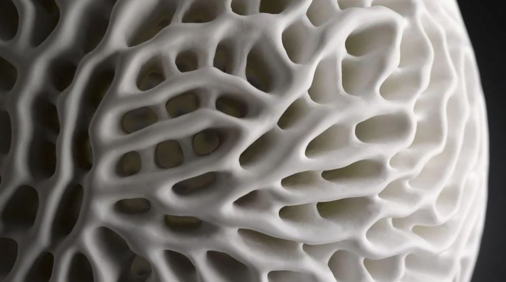 Image source: https://amfg.ai/2019/07/24/7-complex-designs-achieved-with-3d-printing/
Another advantage of additive manufacturing (AM) is its ability to create complex designs that are difficult to achieve with conventional manufacturing methods. Conventional manufacturing techniques, such as milling or lathe, rely on removing undesired parts from a bulk material, making it challenging to create complex designs. In contrast, AM builds objects by adding material layer-by-layer, making it relatively simple to create intricate shapes and structures. This capability of AM allows designers to push the boundaries of what is possible, resulting in more creative and innovative designs that were previously difficult or impossible to manufacture using conventional methods.
What is SLS:
Selective Laser Sintering (SLS) is a form of Laser Powder Bed Fusion (LPBF) that is used in additive manufacturing (AM). In the SLS process, a laser is used to sinter (fuse) powdered material, layer by layer, to build the final 3D printed part. After each layer is printed, a new layer of powder is added to cover the previously printed layer using a recoater. The laser then sinters the powder bed on top of the previous layer, fusing the material together. This process is repeated, layer by layer, until the final part is complete. SLS is a highly versatile and flexible process that can be used with a wide range of materials, making it a popular choice for producing complex, high-quality 3D printed parts.
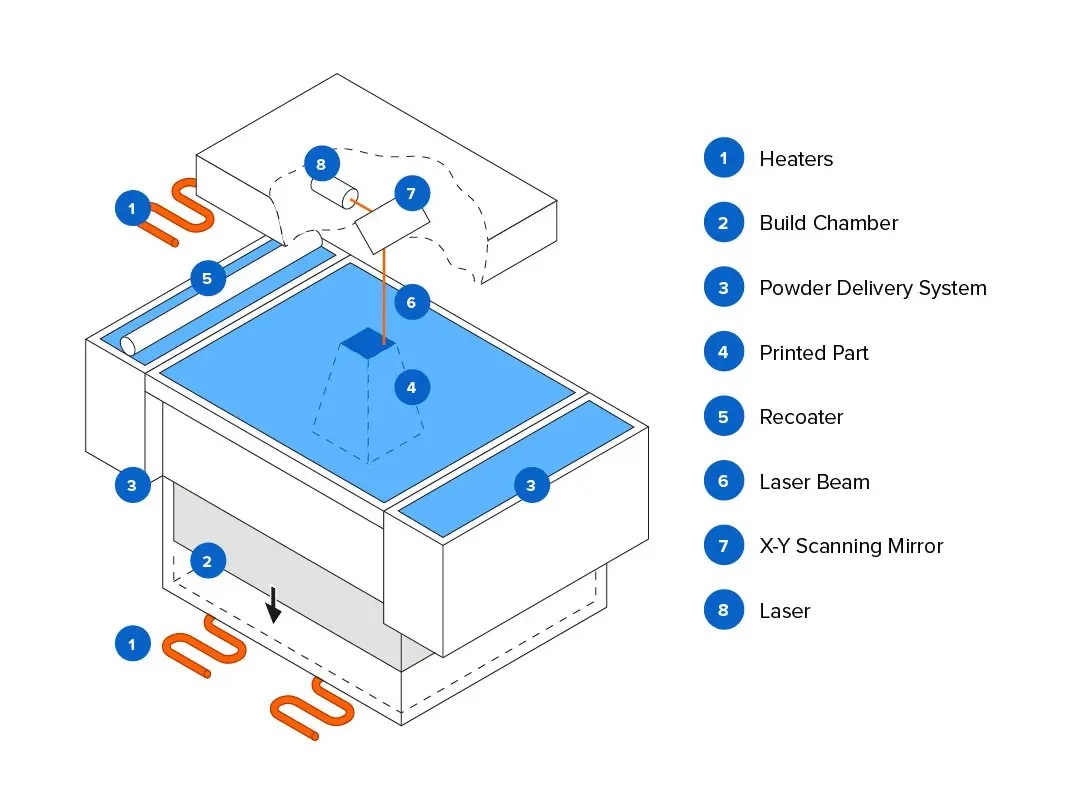
Image source: https://formlabs.com/blog/what-is-selective-laser-sintering/
Problems of traditional SLS:
One of the challenges with traditional Selective Laser Sintering (SLS) is the presence of large heat-affected zones (HAZs) in the substrate. When using continuous wave (CW) or longer pulsed lasers, the beam interacts with the material for a longer time than the thermal diffusion time, resulting in extended irradiation and large HAZs. This can cause thermal damage to the substrate, which can affect the quality and mechanical properties of the final product. However, new techniques and advancements in laser technology have been developed to address this issue and improve the quality of SLS-produced parts.
Advantages of fs laser and challenges:
The main advantages of using femtosecond (fs; 10^-15 second) laser technology in Selective Laser Sintering (SLS) include the ability to create smaller heat-affected zones (HAZs), reducing thermal damage to the substrate. Additionally, the short pulse duration of fs lasers allows for selective heating of only the surface of metal nanopowders (MNPs; metal powders of which the diameter is in nanoscale, 10^-9 meter), without the formation of a liquid phase. This helps to minimize heat shrinkage and distortion, resulting in a more accurate and precise final product. By taking advantage of these benefits, fs laser-based SLS has become a promising approach for producing high-quality, complex 3D printed parts with minimal thermal damage and distortion.
One of the challenges of using femtosecond (fs) laser technology in Selective Laser Sintering (SLS) is the risk of material ablation (removal) due to its high peak power in a short time. When a material absorbs a photon from the laser beam, electrons within the optical penetration depth first absorb the photon energy and become a hot electron gas. When the energy gained by hot electrons is high enough to overcome the work function of the material, the electrons flow out from the surface. This can cause blasting forces from electric charges, such as hot electron blast, Coulomb explosion, or Coulomb repulsion. These processes can lead to ablation of the MNPs by the fs laser, which can affect the quality and integrity of the final product. However, various methods have been developed to mitigate this issue, such as adjusting the laser parameters or modifying the MNPs, enabling the use of fs laser in SLS while maintaining the desired quality and precision.
Our approach to solve the problem:
![]() Figure 1. (a) Energy transfer path in metal NPs after absorbing photons from fs-laser. (b) Electron temperature computed with two temperature model in a single Cu nanoparticle with diameter of 100 nm, at different delay times.
Figure 1. (a) Energy transfer path in metal NPs after absorbing photons from fs-laser. (b) Electron temperature computed with two temperature model in a single Cu nanoparticle with diameter of 100 nm, at different delay times.
To mitigate the risk of material ablation when using femtosecond (fs) laser technology in Selective Laser Sintering (SLS), we propose the use of double-pulse sintering. In our simulation study (Fig. 1b), we observed that the electron temperature increases significantly when the MNP absorbs a single fs laser pulse, which can lead to ablation. By dividing the original single pulse into two shorter pulses and delaying the second pulse, we can reduce the peak electron temperature and avoid ablation. Our simulation results show that the peak electron temperature decreases significantly with the use of double-pulse sintering. By keeping the peak electron temperature below the ablation threshold, we can achieve successful sintering without material ablation, leading to high-quality and precise 3D printed parts.
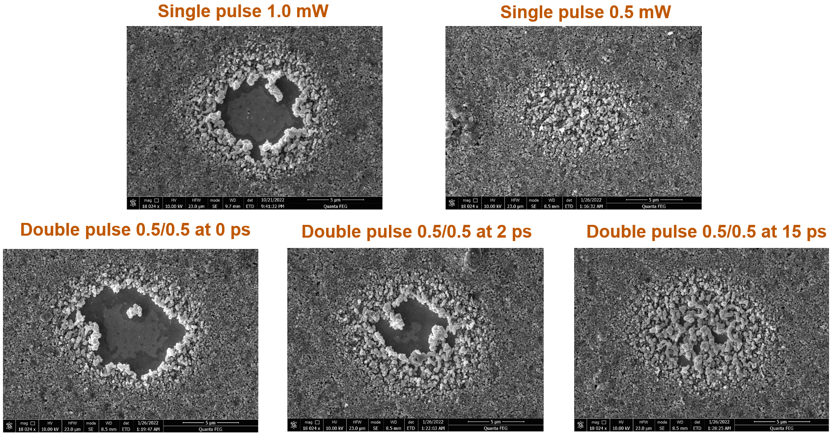 Figure 2. Sintering results of Cu NPs with single and double pulsed fs laser.
We present the spot sintering results in Fig. 2, which demonstrate the effectiveness of our proposed double-pulse sintering method in avoiding material ablation. Our results show that sintering with a single pulse at 1.0 mW intensity is equivalent to sintering with double pulses at 0.5/0.5 mW power and 0 ps delay time (“0.5/0.5” represents double pulses with 0.5 mW + 0.5 mW intensity, and “0 ps” means the delay time of 0 ps). The dark area at the center of the sintered spots represents the ablated area, which is significantly reduced with the use of double-pulse sintering. By increasing the delay time between the two pulses while keeping the same power setup, we observed a further reduction in the ablated area without sacrificing the average power. These results demonstrate the potential of our double-pulse sintering method in achieving high-quality and precise 3D printed parts with reduced risk of material ablation.
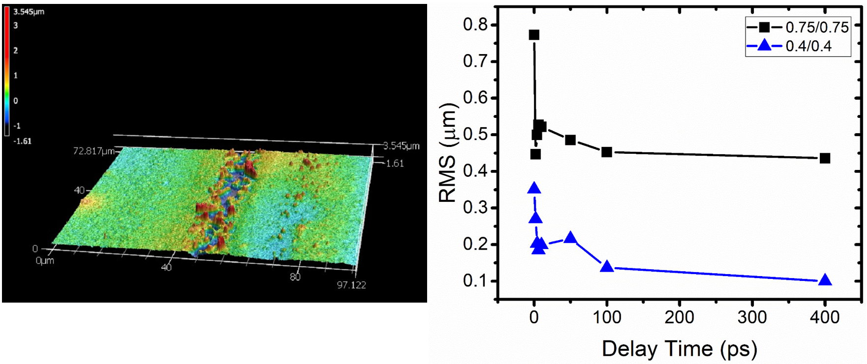 Figure 3. Surface roughness measurement with optical profilometer.
We evaluated the surface roughness of our sintered spots using an optical profilometer, as illustrated in Fig. 3. We plotted the root mean square (RMS) of surface roughness as a function of the delay time between the double pulses, and observed a significant reduction in roughness with increasing delay time. Specifically, we found that the surface roughness decreased rapidly from 0 to 10 ps, which is slightly longer than the electron-phonon coupling time. At a delay time of 10 ps, we observed a 32% decrease in RMS for the 0.75/0.75 power setup, and a 43% decrease for the 0.4/0.4 power setup. These results demonstrate the effectiveness of our double-pulse sintering method in reducing surface roughness and achieving high-quality 3D printed parts.